













- Startseite
- Blogs
- Industry
- What Is a BJT (Bipolar Junction Transistor)? Types, Working Principle, and Applications
What Is a BJT (Bipolar Junction Transistor)? Types, Working Principle, and Applications
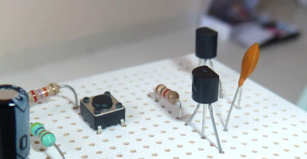
A BJT (bipolar junction transistor) is a three-terminal semiconductor device that controls a large current between its collector and emitter using a much smaller current at its base. Unlike voltage-driven devices, a BJT is a current-controlled component: the base current directly governs the current that flows through the rest of the device.
The bipolar junction transistor belongs to the broader family of transistors and earned its "bipolar" label because it depends on two types of charge carriers: electrons and holes. Available as discrete components or embedded in ICs, BJTs come in two polarities (NPN and PNP) and serve as amplifiers, switches, oscillators, and current regulators across everything from audio equipment to industrial control systems. MOSFETs may dominate headlines, but BJTs still ship in the billions each year, and they outperform their voltage-driven rivals in more applications than most engineers expect.
Key Takeaways
A BJT is a current-controlled, three-terminal semiconductor device that amplifies or switches signals using both electrons and holes as charge carriers.
NPN transistors dominate most circuit designs because of faster switching speed (higher electron mobility) and natural compatibility with ground-referenced logic. PNP transistors fill specific roles in high-side switching and complementary output stages.
The BJT working principle centers on a thin, lightly doped base that lets carriers injected from the emitter reach the collector with minimal recombination, producing current gain (hFE).
Four operating modes (forward active, saturation, cutoff, and reverse active) determine whether the BJT behaves as an amplifier, a closed switch, an open switch, or a rarely-used reverse-gain device.
BJTs retain their edge over MOSFETs in low-voltage switching, audio-quality amplification, current sensing, and ESD-heavy environments.
Selecting a BJT means matching V_CEO, I_C(max), hFE at your actual operating point, and thermal budget to your application, not picking the part with the highest headline gain.
Anatomy of a BJT: Emitter, Base, and Collector
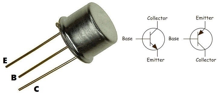
Every bipolar junction transistor consists of three semiconductor regions, each with a specific job and a doping profile to match.
The Emitter
The emitter is the most heavily doped region. Its job is to inject charge carriers (electrons in an NPN, holes in a PNP) into the adjacent base. Heavy doping ensures a flood of carriers crosses the emitter-base junction when that junction is forward-biased.
The Base
The base sits between the emitter and collector, and it's both thin and lightly doped. That combination is deliberate. A thin base means most carriers injected from the emitter will diffuse across without recombining. Light doping keeps the majority carrier count low, so recombination stays minimal. The base region's thinness is what makes transistor action possible. If the base were thick or heavily doped, too many injected carriers would recombine before reaching the collector, and the device would produce no useful gain.
The Collector
The collector occupies the largest physical area. It's moderately doped (lighter than the emitter, heavier than the base) and sits on the opposite side of the base from the emitter. Its role: sweep up the carriers that successfully diffuse through the base. The large junction area helps the collector capture those carriers efficiently, which is why collector current (I_C) makes up the vast majority of emitter current (I_E). A small fraction, typically 1-2% in modern silicon BJTs, recombines in the base and forms the base current (I_B).
Two p-n junctions result from this three-layer sandwich: the emitter-base junction (EBJ) and the collector-base junction (CBJ). How you bias these two junctions determines the transistor's operating mode, its gain, and its behavior in your circuit.
BJT Transistor Symbols: Reading the Schematic
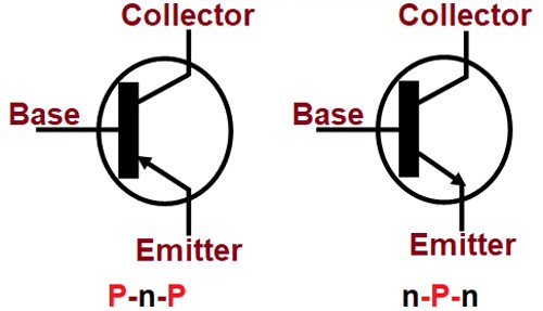
Circuit schematics represent BJTs with a distinct three-terminal symbol, and the difference between NPN and PNP comes down to a single arrow.
NPN Symbol
For an NPN transistor, the emitter arrow points outward, away from the base. A common mnemonic: "Not Pointing iN." That outward arrow indicates conventional current flowing out of the emitter during normal operation. Current enters through the collector, a small portion exits through the base, and the rest exits through the emitter.
PNP Symbol
For a PNP transistor, the emitter arrow points inward, toward the base. Conventional current flows into the emitter, through the device, and exits at the collector. The base still controls the device, but its voltage must be pulled below the emitter voltage to turn it on.
Getting the arrow direction wrong in a schematic will flip every voltage polarity in your bias calculations. The arrow doesn't indicate which terminal connects to ground or supply. It marks the conventional current path at the emitter. Nothing more, nothing less.
How a BJT Works: The Operating Principle
A BJT works like a current valve: a small current flowing into (or out of) the base terminal controls a much larger current flowing between the collector and emitter. That's the BJT working principle in one sentence.
The ratio between collector current and base current defines the device's DC current gain, written as hFE or beta. A BJT with an hFE of 200 lets 1 mA of base current support 200 mA of collector current. That gain is what makes the BJT useful as an amplifier. It's also what makes it work as a switch: push enough base current to saturate the device, and the collector-emitter path conducts with minimal voltage drop.
Carrier Flow in an NPN Transistor
Forward-bias the emitter-base junction (apply roughly 0.6-0.7 V to the base relative to the emitter) and reverse-bias the collector-base junction (keep the collector voltage higher than the base). Here's what happens inside:
The heavily doped n-type emitter injects electrons into the thin p-type base. Because the base is so thin (on the order of a few hundred nanometers in modern devices), most electrons don't recombine with holes. Instead, they diffuse across the base and reach the collector-base depletion region. The electric field of the reverse-biased junction then sweeps those electrons into the n-type collector.
A small number of electrons do recombine in the base, and that recombination creates I_B. The external base circuit supplies replacement holes to sustain this process. The result: I_E = I_C + I_B, where I_C dwarfs I_B by a factor of hFE.
How a PNP Transistor Differs
A PNP transistor runs on identical physics with reversed carrier roles and voltage polarities.
The p-type emitter injects holes (not electrons) into the thin n-type base. Those holes diffuse through and get swept into the p-type collector. To turn on a PNP BJT, the base voltage must sit below the emitter voltage by about 0.6-0.7 V. Conventional current flows into the emitter and out through the collector.
That current direction means PNP transistors work well in high-side switching configurations, where the load connects between the transistor and ground. NPN transistors, by contrast, sit on the low side with the load above them.
One more practical difference: holes have lower mobility than electrons in silicon (roughly 3x lower). That gap gives NPN transistors faster switching speeds and higher f_T values at the same geometry. For speed-critical designs, NPN is the default choice.
NPN vs PNP: Choosing the Right BJT Type
Both NPN and PNP fall under the BJT branch of the wider transistor type family, but the practical differences between them matter more for design decisions than the textbook layer diagrams.
| Feature | NPN Transistor | PNP Transistor |
| Majority carriers | Electrons | Holes |
| Turn-on condition | V_BE ≈ +0.7 V | V_EB ≈ +0.7 V |
| Conventional current flow | Into collector, out of emitter | Into emitter, out of collector |
| Typical circuit position | Low-side (load above, transistor to ground) | High-side (transistor to supply, load below) |
| Relative switching speed | Faster (higher electron mobility) | Slower (~3x lower hole mobility) |
| Common use case | Ground-referenced logic, digital switching, most amplifier stages | Power supply switching, level shifting, complementary pairs |
NPN transistors show up more often in designs for a reason. Most digital logic operates with ground as the reference, and NPN devices sink current to ground. A positive signal at the base turns the transistor on. PNP transistors need a base voltage lower than the emitter, which can complicate drive circuitry when your control signal is ground-referenced.
Where PNP transistors earn their place is in push-pull output stages (paired with an NPN for complementary operation) and circuits that switch the positive rail. Audio power amplifiers use NPN/PNP complementary pairs in the output stage to push and pull current through the speaker in both halves of the signal cycle.
Operating Modes of a BJT
A BJT has four operating modes, set by how the two junctions are biased. Three of them matter for circuit design; the fourth rarely gets used intentionally.
| Mode | Emitter-Base Junction | Collector-Base Junction | Behavior |
| Forward active | Forward-biased | Reverse-biased | Linear amplification; I_C = hFE × I_B |
| Saturation | Forward-biased | Forward-biased | Fully on, closed switch; V_CE ≈ 0.2 V |
| Cutoff | Reverse-biased (or unbiased) | Reverse-biased | Fully off, open switch; I_C ≈ 0 |
| Reverse active | Reverse-biased | Forward-biased | Reverse conduction; poor gain; rarely used |
Forward Active
This is where amplification happens. Collector current tracks base current proportionally, and the transistor operates in its linear region. Audio amplifier stages, sensor conditioning circuits, and active filters all depend on this mode.
Saturation
Both junctions are forward-biased, and the collector-emitter voltage drops to 0.2-0.3 V. The BJT transistor behaves like a closed switch. Designers pick this mode when they need the transistor to connect a load to the circuit with minimal voltage drop.
Cutoff
No base current flows (or V_BE sits below the ~0.6 V threshold), so collector current drops to near zero. The transistor acts as an open switch, and the full supply voltage appears across collector-emitter.
Switching circuits alternate between saturation and cutoff; amplifier circuits hold the BJT in forward active mode. That's the operating mode decision in its most distilled form.
Reverse Active
The collector acts as emitter and vice versa. The device still conducts, but gain (beta_R) is far lower than forward active. You won't encounter this in typical designs.
Key BJT Parameters for Datasheet Reading
Not every datasheet spec carries equal weight. These are the parameters that shape real design decisions.
DC Current Gain (hFE)
Measures how many milliamps of collector current you get per milliamp of base current. A device with hFE = 300 at I_C = 150 mA needs only 0.5 mA of base drive to reach that collector current. But hFE isn't fixed. It varies with temperature, collector current, and collector-emitter voltage. The Toshiba 2SC4793(F,M), for example, specifies hFE ranges across different I_C values, and the gain at your actual operating point may differ from the headline figure. Always check the gain curves, not just the maximum rating.
Maximum Collector Current (I_C(max))
The upper limit on continuous current through the collector. Exceed it, and you risk overheating the die or degrading the device. Your load current plus a safety margin should sit well under this rating.
Collector-Emitter Breakdown Voltage (V_CEO)
The highest voltage the device can block when the base is open. Your supply voltage plus any inductive spikes must stay below this number.
Saturation Voltage (V_CE(sat))
The residual voltage across collector and emitter when the transistor is fully on. Lower is better for switching efficiency. Typical values fall between 0.1 V and 0.3 V, depending on collector current and base drive.
Base-Emitter Turn-On Voltage (V_BE(on))
Sits around 0.6-0.7 V for silicon BJTs. It shifts with temperature (roughly -2 mV/°C), which matters in precision analog designs.
Transition Frequency (f_T)
The frequency at which current gain drops to unity. For audio circuits, a few MHz is plenty. RF work demands hundreds of MHz or more.
These parameters interact. Higher I_C pushes V_CE(sat) up and can reduce hFE. Higher temperatures increase I_C for a given bias, a positive feedback loop that can lead to thermal runaway without proper stabilization. Read parameters as a system, not as isolated numbers.
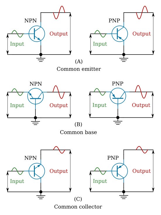
Common BJT Circuit Configurations
Three standard configurations exist for a BJT, each trading off gain, impedance, and bandwidth differently.
Common Emitter (CE)
The workhorse. The emitter connects to signal ground (often through a degeneration resistor for stability), the input drives the base, and the output appears at the collector. This arrangement delivers both voltage gain and current gain. The trade-off: 180° phase inversion and bandwidth limited by the Miller effect at the collector-base junction.
Common Base (CB)
The base ties to signal ground. Input feeds the emitter, output comes from the collector. Current gain sits near unity, but voltage gain can be high, and the configuration excels at high frequencies because the grounded base shields the input from output capacitance. RF amplifiers and cascode stages lean on this topology.
Common Collector (Emitter Follower)
The collector connects to the supply rail, and the output is taken from the emitter. Voltage gain is approximately 1 (the output "follows" the input), but current gain is high and output impedance is low. That makes it a natural buffer between a high-impedance source and a low-impedance load.
BJT Applications: Where Bipolar Transistors Still Win
MOSFETs dominate power switching and digital logic. No secret there. But bipolar junction transistors hold distinct advantages in several application areas, and knowing those niches helps you pick the right device instead of defaulting to whatever seems popular.
Audio Amplification
Bipolar transistors exhibit better linearity in their active region compared to MOSFETs, and their 1/f noise (flicker noise) is lower. For audio preamplifiers and headphone drivers where signal fidelity matters at low frequencies, BJTs deliver cleaner output. Many high-end audio amplifier designs still use discrete BJT output stages with NPN/PNP complementary pairs for this reason.
Low-Voltage Switching
BJTs turn on at roughly 0.7 V base-emitter. A MOSFET needs a gate-threshold voltage that can range from 1 V to 4 V, limiting its usefulness in coin-cell-powered circuits or low-voltage sensor outputs. A part like the ROHM 2SD1733TLR, an NPN BJT in a compact SOT-23 package, can switch small loads directly from low-voltage logic signals without a gate driver.
Current Mirrors and References
The predictable V_BE vs. I_C relationship in BJTs makes them ideal for current mirrors. Two matched BJTs on the same die track each other's collector current across temperature, and analog IC designers still build current sources from BJT pairs for exactly that reason. This same principle powers bandgap voltage references found in most power management ICs.
Voltage Regulation
Linear regulators often use a BJT as the pass element. Low saturation voltage means less dropout between input and output, and the base-driven control loop responds fast enough for stable regulation.
RF and High-Frequency Circuits
Specialized BJTs (and their heterojunction cousins, HBTs) achieve transition frequencies well above 10 GHz. Cell phone front-ends, GPS receivers, and Wi-Fi modules still use BJT-based low-noise amplifiers for the first gain stage.
ESD-Resistant Environments
Bipolar transistors tolerate electrostatic discharge better than MOSFETs, whose thin gate oxides can punch through under voltage spikes. Industrial control equipment, automotive sensors, and field-deployed instrumentation often specify BJTs partly for this ruggedness.
A full BJT vs MOSFET comparison deserves its own dedicated discussion, but the short version: BJTs win on low-voltage turn-on, analog linearity, noise performance, and ESD tolerance. MOSFETs win on gate drive simplicity (no DC current needed), switching speed at higher voltages, and on-resistance scaling. The IGBT bridges both worlds by combining a MOSFET gate with a BJT output stage for high-power switching.
How to Select the Right BJT for Your Design
Picking a BJT from a discrete semiconductor catalog goes beyond matching a part number to a schematic symbol. Here's a parameter-driven approach.
1. Define the application: amplifier or switch? An amplifier application means you'll care most about hFE linearity, f_T, noise figure, and bias stability. A switching application puts V_CE(sat), switching time, and maximum I_C at the top of the list.
2. Set your voltage headroom. Your supply voltage plus any transient spikes (inductive loads, motor back-EMF) must stay below the BJT's V_CEO rating. A 2x safety factor over nominal supply voltage is a solid starting point.
3. Calculate your current requirements. Your load current dictates the minimum I_C(max) rating. For switching, also account for inrush current and calculate the base current needed for saturation: I_B(sat) = I_C / hFE(min). Use the minimum guaranteed hFE from the datasheet, not the typical value.
4. Evaluate hFE at your operating point. The gain on the front page of a datasheet is often the maximum at an ideal operating point. Your circuit won't run there. Check the hFE vs. I_C curve at your actual collector current, something you can verify across single BJT datasheets before ordering samples. A device rated at hFE = 400 might drop to 80 at higher currents.
5. Thermal budget and package selection. Multiply V_CE by I_C to get power dissipation. Compare that against the package's thermal resistance (R_θJA) and your maximum ambient temperature. SOT-23 packages work for low-power signal switching. TO-220 or TO-247 handles watts of dissipation with a heatsink. A device like the ROHM 2SD1898T100R in a small-footprint package suits low-to-mid-power designs where board space is tight.
6. Consider pre-biased BJTs for simpler designs. If your switching circuit runs at a fixed logic voltage and predictable load, a pre-biased (digital) BJT comes with integrated base and base-emitter resistors. You lose some bias flexibility, but for standard microcontroller-driven switching tasks, eliminating two external components and simplifying the BOM is worth the trade-off.
7. Check complementary pair availability. Push-pull output stages, H-bridges, and Class AB amplifiers need matched NPN/PNP pairs. Confirm that a complementary device with similar hFE, V_CEO, and I_C(max) specs exists from the same manufacturer. Mismatched pairs cause crossover distortion and thermal imbalance.

FAQs
Articles you may also like
Design of High Current H-Bridge Motor Drive Circuit

The working principle, key parameters, and selection of TVS

Understanding NAND Gate: The Universal Logic Gate in Digital Circuits
Gas Discharge Tube Symbols, Characteristics and Structure

-
-
-
-
-

-
microchip-technology
I2C, 2-Wire Serial Real-Time Clock IC with Battery-Backed SRAM and EEPROM
-
-
-