













- Home
- Blogs
- Semiconductor
- What Is a MOSFET Transistor? Working Principle, Types, and Applications
What Is a MOSFET Transistor? Working Principle, Types, and Applications
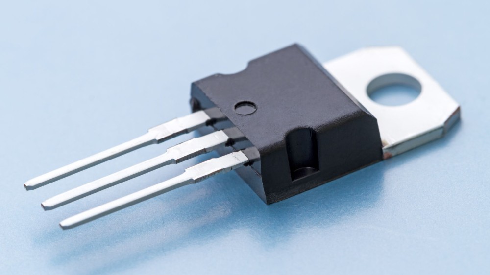
MOSFET stands for Metal-Oxide-Semiconductor Field-Effect Transistor. That's a mouthful, so here's what it actually means in plain English.
A MOSFET transistor controls electrical current using voltage, not current. No base current flows constantly, no wasted power keeping the gate alive. You apply voltage to the gate terminal, a channel opens between drain and source, and current flows. Remove the voltage, the channel closes. It's that direct.
Nearly every electronic device you touch relies on MOSFETs. Your phone's processor packs billions of them. Your laptop's power supply switches them thousands of times per second. Even your car's headlight controller probably runs through one. If you're working with transistors at any level, knowing how MOSFETs work isn't optional.
What's Inside a MOSFET? Pin by Pin
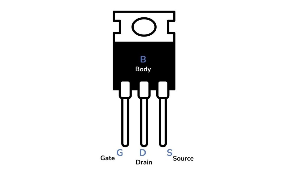
Four terminals make up every MOSFET: Gate (G), Drain (D), Source (S), and Body (B). Most discrete packages tie the body to the source internally, so you'll usually interact with just three pins.
Here's what each does:
G Gate controls the on/off state. It sits on top of a thin silicon dioxide (SiO₂) insulating layer, which is why the gate draws almost zero current at DC. That insulation is the "oxide" in Metal-Oxide-Semiconductor.
D Drain is where the current exits the device (in N-channel types) and connects to your load.
S Source is the reference terminal. Gate voltage is measured relative to the source, written as V_GS.
B Body/Substrate affects threshold voltage through the body effect (a bias-dependent voltage shift). In most circuits, you won't worry about it because it's shorted to the source.
One big structural difference separates MOSFETs from BJTs. A BJT requires a continuous base current to stay on. A MOSFET gate, insulated by oxide, requires charge to turn on but draws no steady-state current. That single difference is why MOSFETs dominate digital circuits and power electronics. For a broader look at how different types of transistors compare, and where BJTs still win, check our companion article. Cover the BJT vs MOSFET tradeoffs in a dedicated piece.
How Does a MOSFET Work?
The operating principle comes down to electric fields, not current injection.
When you apply a positive voltage to the gate of an N-channel MOSFET (relative to the source), that voltage creates an electric field across the thin oxide layer. This field attracts electrons from the P-type substrate and pulls them toward the surface, right underneath the gate. Once enough electrons accumulate, they form a conductive channel between the drain and source regions.
The minimum gate-to-source voltage needed to create this channel is called the threshold voltage (V_th). Below V_th, the MOSFET stays off. Above it, current starts flowing.
Three operating regions determine how the device behaves:
Cutoff: V_GS sits below V_th. No channel forms, no current flows. The MOSFET acts like an open switch.
Linear (Ohmic/Triode): V_GS exceeds V_th, and the channel is fully formed. Current through the device increases proportionally with drain-to-source voltage (V_DS). The MOSFET behaves like a voltage-controlled resistor here, and this is the region you want when using a MOSFET switch because R_DS(on) drops to milliohms in a good power device.
Saturation: V_DS climbs high enough that the channel pinches off near the drain. Current levels out and stays roughly constant regardless of V_DS increases. Amplifier circuits operate in this region because small gate voltage changes produce proportional current changes.
N-Channel or P-Channel? How to Choose
MOSFET transistors are split into two families based on what carries the current.
N-Channel MOSFET
Electrons do the work. Since electrons move about 3x faster through silicon than holes, N-channel MOSFETs deliver lower on-resistance, faster switching, and smaller die sizes for equivalent current ratings. That's why you'll find them in the majority of power supply designs, motor drivers, and digital logic.
An N-channel device turns on when V_GS goes positive above the threshold. For low-side switching (source connected to ground), driving the gate is straightforward: apply a positive voltage from your microcontroller or driver IC.
Popular examples: Infineon's IRLZ44N, a logic-level N-channel MOSFET rated at 55V and 47A with a gate threshold low enough for 5V logic. Vishay's SQ1912AEE offers another option for compact, surface-mount designs.
P-Channel MOSFET
Holes, not electrons, carry the current here. A P-channel MOSFET turns on when the gate goes negative relative to the source. You'll see P-channel devices in load switches, reverse polarity protection circuits, and battery disconnect applications where simplicity matters more than squeezing every milliohm out of R_DS(on).
The tradeoff? Higher on-resistance for the same die area compared to the N-channel. So P-channel parts tend to show up in lower-current circuits where fewer board components and faster design cycles beat raw efficiency.
Nexperia's BSS84AKS is a compact P-channel MOSFET well-suited for low-power high-side switching in battery-operated devices.
Enhancement Mode vs. Depletion Mode
Most MOSFET transistors you'll encounter are enhancement mode. Normally off. Apply gate voltage to turn them on. This is the "normally open switch" behavior.
Depletion mode works the opposite way. The channel exists at zero gate bias, and you apply a voltage to pinch it off. These show up in niche roles like constant-current sources and fail-safe power paths, but they're uncommon in general-purpose designs.
Decoding the MOSFET Symbol on a Schematic
Reading a MOSFET symbol takes about five seconds once you know two rules.
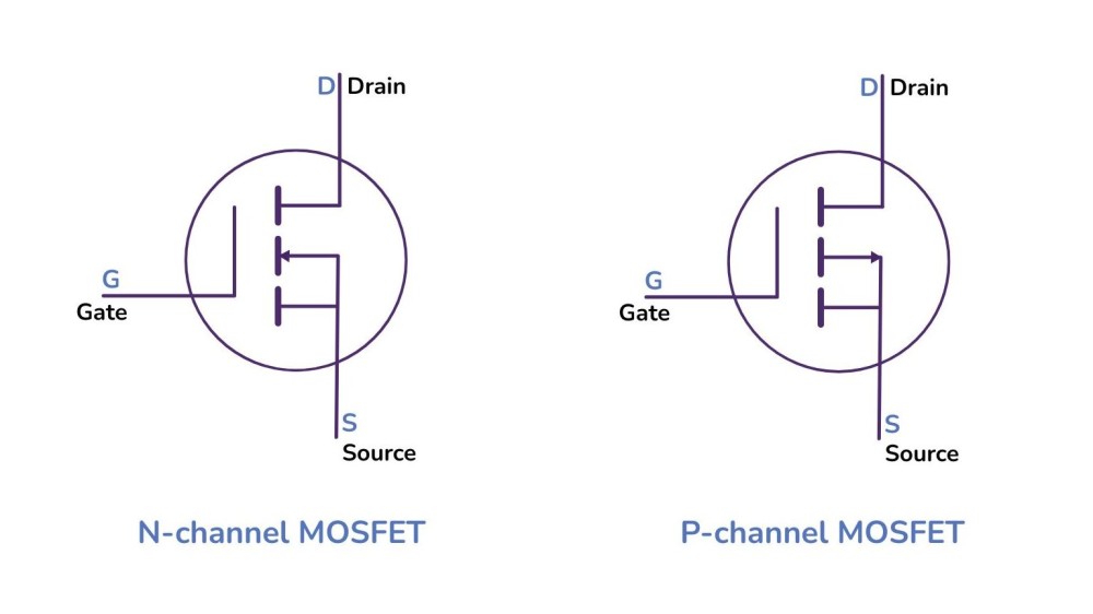
Rule 1: Check the arrow direction
Arrow pointing inward, toward the channel? That's an N-channel device (current flows from drain to source).
Arrow pointing outward, away from the channel? P-channel (current flows from source to drain).
Rule 2: Check the channel line
A dashed or broken line between drain and source = enhancement mode.
A solid, continuous line = depletion mode.
Think of it this way: a broken line means the channel doesn't exist yet (no path until you apply gate voltage), and a solid line means the channel is already there.
The gate connects to a vertical bar separated from the channel by a visible gap. That gap represents the oxide insulation. Some symbols include a fourth terminal (body), shown connected to the source or drawn separately.
So when you spot a MOSFET on a schematic, find the arrow, check the line style, and you've identified the device type in two steps.
Using a MOSFET as a Switch
A MOSFET switch toggles between two states: fully off (cutoff) and fully on (linear region with minimal R_DS(on)). No in-between. You don't want it lingering in saturation during switching because that's where power gets burned as heat.
Low-Side Switching (N-Channel)
Connect the source to ground. Place the load between the positive supply and the drain. Drive the gate high to turn on. This is the most common configuration because gate drive is simple. Your microcontroller's 3.3V or 5V output can handle it directly for logic-level MOSFETs.
Add a 10k-100k pull-down resistor from gate to source. Why? Without it, the gate floats when your controller pin goes high impedance (during boot-up, for example), and a floating gate can turn the MOSFET on unexpectedly. That resistor keeps the default state "off."
High-Side Switching (P-Channel)
Connect the source to the positive supply rail. Load goes between drain and ground. To turn on a P-channel MOSFET, pull the gate below the source voltage. Pulling it to ground works when V_supply doesn't exceed the device's V_GS(max) rating, which caps at -20V for most P-channel parts.
Above 20V supply rails, a level-shifting circuit keeps the gate voltage within safe limits. A common trick: use an NPN transistor with its collector tied to the MOSFET gate through a pull-up resistor to the source. When the NPN turns on, it pulls the gate low; when the NPN turns off, the resistor pulls the gate back to the source, turning the MOSFET off.
When Switching Speed or Voltage Gets Serious
High-frequency PWM (above ~50 kHz), half-bridge topologies, and voltages over 100V call for dedicated gate driver ICs. The reason for this? Gate capacitance. Every MOSFET gate looks like a small capacitor (measured as total gate charge, Q_g), and charging that capacitor fast enough for clean switching requires more current than a microcontroller pin delivers.
For high-voltage power conversion and EV inverter designs, SiC (silicon carbide) MOSFETs like the CAS120M12BM2 from Wolfspeed handle 1200V with switching characteristics that silicon can't match. The difference between JFET and MOSFET in switching behavior becomes relevant at these performance levels.
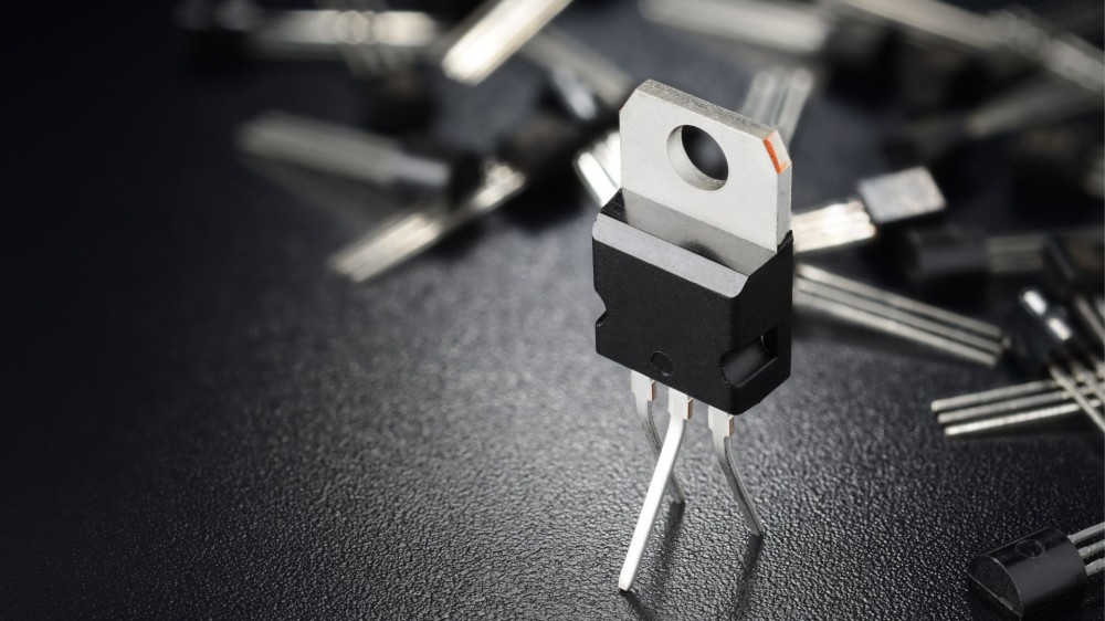
What a Gate Driver Does Inside a Switching Cycle?
A MOSFET gate driver does more than just provide voltage. It fights the Miller plateau.
When you charge a MOSFET gate, the voltage doesn't rise smoothly. It climbs, then stalls at a flat spot (the Miller plateau) where all the driver's current goes toward charging the gate-drain capacitance (C_gd) as the drain voltage swings. Until the driver pushes through this plateau, the MOSFET sits in its highest-loss state, partially on, burning power as heat. A weak driver lingers here. A strong driver punches through it in nanoseconds.
That's why gate driver ICs spec peak source/sink currents of 1A, 4A, even 9A.
The formula: I_drive = Q_g / t_switch.
A MOSFET with 40 nC of gate charge switching in 40 ns demands about 1A peak.
For high-side N-channel drives, the bootstrap circuit inside most driver ICs charges a small capacitor (typically 100 nF to 1 µF) during the low-side on-time, then uses that stored energy to lift the gate voltage above the supply rail during the high-side on-time. If your duty cycle stays too high for too long, the bootstrap cap drains, and the high-side MOSFET drops out. Some drivers include internal charge pumps to handle 100% duty cycle.
What is a MOSFET used for?
Anywhere you need to switch or regulate electrical power efficiently.
➧DC-DC power conversion. Buck, boost, and flyback converters all depend on MOSFETs switching at 100 kHz to several MHz. Lower R_DS(on) and lower gate charge directly translate to higher converter efficiency.
➧Motor control. Four MOSFETs in an H-bridge drive DC motors forward and reverse. PWM signals on the gates control speed without the energy waste of a rheostat.
➧Digital logic and processors. Every CMOS gate pairs an N-channel and a P-channel MOSFET. A 3nm-node processor packs billions of FinFET and gate-all-around (GAA) transistor structures, all descendants of the basic MOSFET.
➧LED lighting. MOSFETs switch LED arrays, and PWM dimming through a MOSFET controls brightness without color shift or efficiency loss.
➧Automotive systems. Battery management, headlight drivers, electric power steering, and EV traction inverters. Automotive-grade MOSFETs carry an AEC-Q101 qualification for reliability under harsh conditions.
➧Audio. Class-D amplifiers push MOSFET switching into the ultrasonic range (300-500 kHz), delivering 90%+ efficiency where Class-AB designs top out around 60%.
Find MOSFET transistors for your project at Dyethin, with datasheets, pricing, and stock availability.
FAQs
Articles you may also like
Characteristics of CPU, GPU, and FPGA
Silicon controlled rectifier (SCR) and switch control circuit explained
Accurately measure resistor value using ADC
The difference between RAM ROM FLASH