


- Home
- Featured Products
- Analog Devices
- MAX485 is an RS 485/RS422 transceiver integrated circuit IC produced
MAX485 is an RS 485/RS422 transceiver integrated circuit IC produced
MAX485 is a commonly used RS485/RS422 transceiver integrated circuits, this article will explain the chip through the actual use of cases and disadvantages.
What is the transceiver IC MAX485?
The MAX481, MAX483, MAX485, MAX487–MAX491, and MAX1487 are low-power transceivers for RS-485 and RS422 communication. Each part contains one driver and one receiver. The MAX483, MAX487, MAX488, and MAX489 feature reduced slew-rate drivers that minimize EMI and reduce reflections caused by improperly terminated cables,thus allowing error-free data transmission up to 250kbps.
The driver slew rates of the MAX481, MAX485, MAX490,MAX491, and MAX1487 are not limited, allowing them to transmit up to 2.5Mbps.
These transceivers draw between 120µA and 500µA of supply current when unloaded or fully loaded with disabled drivers. Additionally, the MAX481, MAX483, and MAX487 have a low-current shutdown mode in which they consume only 0.1µA. All parts operate from a single 5V supply.
Drivers are short-circuit current limited and are protected against excessive power dissipation by thermal shutdown circuitry that places the driver outputs into a high-impedance state. The receiver input has a fail-safe feature that guarantees a logic-high output if the input is open circuit.
The MAX487 and MAX1487 feature quarter-unit-load receiver input impedance, allowing up to 128 MAX487/MAX1487 transceivers on the bus. Full-duplex communications are obtained using the MAX488–MAX491, whilethe MAX481, MAX483, MAX485, MAX487, and MAX1487 are designed for half-duplex applications.
Characteristics of Transceiver IC MAX485
From the MAX485 Datasheet, it can be inferred that MAX485 has the following characteristics
Compliant with RS 485 and RS422 standards
Half duplex communication mode
High speed data transmission: up to 10Mbps
Wide common mode voltage range: -7V to+12V
High resistance to electromagnetic interference (EMI)
Low power consumption: typical value of 1.5mA in normal operating mode
Driver short circuit and thermal shutdown protection function
Packaging form: DIP or SOIC, etc

MAX485 real image
The application range of MAX485
MAX485 Datasheet user manual guide, the application scope of IC 485 includes
Low-Power RS-485 Transceivers
Low-Power RS-422 Transceivers
Level Translators
Transceivers for EMI-Sensitive Applications
Industrial-Control Local Area Networks
MAX485 is widely used in industrial automation, building automation, security monitoring, intelligent transportation and other fields, especially in situations that require long-distance transmission, multi-point communication, or high anti-interference ability.
MAX485 Pinout arrangement

MAX485 pinout
MAX485 pinout Description:
A. B: Differential signal line, used for data transmission.
DE, RE: Driver enable and receiver enable control pins.
DI: Data input pin, used to send data to the bus.
RO: Data output pin, used to receive data from the bus.
VCC, GND: power and ground pins.
| PIN | NAME | FUNCTION | ||||
| MAX481/MAX483/ MAX485/MAX487I MAX1487 | MAX488/ MAX490 | MAX489/ MAX491 | ||||
| DIP/SO | μMAX | DIP/SO | μMAX | DIP/SO | ||
| 1 | 3 | 2 | 4 | 2 | RO | Receiver Output: If A > B by 200mV,RO will be high; If A |
| 2 | 4 | 一 | 3 | RE | Receiver Output Enable.RO is enabled when RE is low; RO is high impedance when RE is high. | |
| 3 | 5 | 4 | DE | Driver Output Enable.The driver outputs,Y and Zare enabled by bringing DE high. They are high impedance when DE is low. If the driver outputs are enabled,the parts function as line drivers. While they are high impedance,they function as line receivers if RE is low. | ||
| 4 | 6 | 3 | 5 | 5 | DI | Driver Input.A low on DI forces output Y low and output Z high. Similarly,a high on DI forces output Yhigh and output Z low. |
| 5 | 7 | 4 | 6 | 6,7 | GND | Ground |
| 5 | 7 | 9 | Y | Noninverting Driver Output | ||
| 6 | 8 | 10 | Z | Inverting Driver Output | ||
| 6 | 8 | A | Noninverting Receiver Input and Noninverting Driver Output | |||
| 一 | 8 | 2 | 12 | A | Noninverting Receiver Input | |
| 7 | 1 | - | B | Inverting Receiver Input and Inverting Driver Output | ||
| 7 | 1 | 11 | B | Inverting Receiver Input | ||
| 8 | 2 | 1 | 3 | 14 | Vcc | Positive Supply: 4.75V≤Vcc≤5.25V |
| 1,8,13 | N.C. | No Connect-not internally connected | ||||
MAX485 pinout data comes from MAX485 Datasheet
Usage of MAX485
Choose the appropriate communication rate and terminal resistance as needed.
Connect wires A and B to the bus and ensure the correct connection of the differential signal lines.
Switch the sending and receiving modes through the DE and RE control pins.
Input data from the DI pin and output it from the RO pin.
As needed, suitable decoupling capacitors can be added between VCC and GND.
MAX485 usage tips
When transmitting over long distances, it is recommended to use twisted pair cables as differential signal lines to improve anti-interference capabilities.
Add terminal resistors (usually 120 Ω) at both ends of the bus to match the line impedance and improve signal quality.
When multiple devices are connected on the same bus, ensure that each device's address is unique to avoid conflicts.
When designing a PCB, keep the length of the differential signal line consistent to reduce signal distortion.
To ensure the stability of the circuit, it is recommended to add decoupling capacitors between VCC and GND.
MAX485 Advantages and Disadvantages
Advantages:
Long distance transmission capacity: up to 1200 meters (using twisted pair cables).
High anti-interference ability: differential signal transmission method.
Multipoint communication capability: Supports up to 32 nodes.
High speed data transmission: up to 10Mbps.
Wide common mode voltage range: suitable for various application scenarios.
Equipped with driver short circuit and thermal shutdown protection functions, improving circuit reliability.
Disadvantages:
Half duplex communication mode: cannot perform both sending and receiving operations simultaneously.
When multiple devices send data simultaneously, it may lead to conflicts and data loss.
For certain high-speed applications, external components may be required for stability compensation.
For certain specific applications, there may be electromagnetic interference issues.
RS485 automatic transceiver circuit
As for the MAX485 module, everyone is familiar with it. Would you design a MAX485 module circuit that can also have its own transceiver function? Or you can simply find a circuit or even use it without considering its principles. The MAX485 module generally relies on microcontroller control, so development boards such as STM32 microcontrollers usually have RS485 modules on them, because the MAX485 module only requires your MCU to have a serial port
After analyzing the circuit diagrams of several STM32 development boards on the market regarding the MAX485 module, it was found that the circuit design of the MAX485 module is almost identical


It can be found that there are only two types of chips commonly used in the 485 communication module, SP3485 and MAX485, and the schematic diagrams are similar.
Traditional RS485 circuit
Both SP3485 and MAX485 have the same circuit

First, let me explain the principle: because microcontroller communication is usually at TTL level, and if our external equipment is a 485 device, the communication level is at 485 level. The levels of these two are different, so they cannot be directly connected together. We need a level conversion chip in the middle to negotiate, so we have our 485 chip. Because 485 communication is half duplex, which means that data cannot be received simultaneously when sending data, we also refer to the 485 chip as a half duplex transceiver. The SP3485 chip is a very classic low-power half duplex transceiver that meets the requirements of RS-485 serial protocol.
Then the pins of this chip are defined as follows:
● RO receiver output
● RE receiver output enable (effective at low level)
● DE - Driver output enable (effective at high level)
● DI driver input
● GND connected to ground
● A - Driver output/receiver input (in phase)
● B - Driver output/receiver input (reverse phase)
● VCC - chip powered
Do you have any questions now? How is this pin called a receiver or an output? A real person asked this question. Generally, when data from 485 devices is sent to the MCU, we call the chip a receiver because it receives external data. When the MCU sends data to 485 devices, we call the chip a driver because at this point it seems like we are driving the chip to send data outward.
The driver output of SP3485 is differential output, and the output voltage during no-load is 0V~+3.3V. SP3485 has an enable control line (effective at high levels). The logic high level (1) on DE will enable the differential output of the driver.
The input of the SP3485 receiver is differential input, and the input resistance of the receiver is usually 15K. If RE is low, the receiver is enabled, otherwise the receiver is disabled.
This leads to a conclusion
● ED: 1 transmission enable; 0 Send Prohibited
● RE: 0 receive enable; 1. Reception prohibition
Therefore, we usually connect ED and RE together, and when the microcontroller MCU sends data to the outside, it will use USART_ EN set to 1, when the microcontroller MCU receives external data transmission, it will use USART_ Setting EN to 0 is sufficient.
Of course, when we write programs, it can be relatively troublesome because we need to include USART in both receiving and sending_ The EN pin is set at different levels.

Is there a circuit that can automatically transmit and receive data?
The answer is yes, as long as we add a transistor on top of this circuit, we can solve it.
Automatic switching of RS485 circuit for transmitting and receiving

Everyone, let's see that we have added a classic transistor switch circuit on top of the previous circuit. A typical transistor switching circuit is composed of resistor R6, resistor R7, and NPN transistor Q1. R7 is a current limiting resistor, preferably 4.7K or 10K. R6 is an pull-up resistor, which can be selected as either 4.7K or 10K.
As we all know after studying analog electronics, NPN transistors have high-level conduction. When TX is at a high level, the transistor conducts, and the RE and DE pins are grounded, entering reception mode. When TX is at a low level, the transistor is cut off, and the RE and DE pins are connected to a high level to enter transmission mode.
Questions?
The DI pin was originally connected to TX, but now it is directly grounded. Isn't it because all the data sent is 0? Can it work normally?
Answer: Of course you can!
Sending data process
Sending data uses the TX pin of the microcontroller, which means displaying data on the TX pin. To send data 0x32, written as binary, it means 0x001100110. The TXD pin will sequentially display 1 and 0 with high and low levels.
When TX sends 0, the transistor is not conducting and the DE is connected to a high level, entering the transmission mode. The 485 chip will reflect the level on the DI to the AB pin for output, because the DI is already grounded, the AB pin will transmit 0. So, when TXD sends 0, AB pin sends 0.
When TX sends 1, the transistor conducts and RE is connected to a low level, entering the receiving mode. The AB pin of the 485 chip enters a high resistance state because R3 pulls A high and R2 pulls B low. Therefore, AB transmits 1. So, when TXD sends 1, AB pin sends 1.
In one sentence: TXD sends 1, AB sends 1; TXD sends 0, AB sends 0.
Receiving data process
Receive data using the microcontroller pin RX, and display data on the RXD pin. During the process of receiving data, the TX pin remains at a high level. When TXD is at a high level and RE is at a low level, it becomes a receiving state. Then, the RO pin of the 485 chip (i.e. the pin connected to RX) will receive the data transmitted by AB.
How magical!
Is there a chip that can automatically switch between sending and receiving functions? The answer is yes.
Automatic direction switching chip-MAX13487
In order to overcome the uncertainty of direction control caused by software participation, Meixin Company has released the first RS485 chip that claims to support automatic chip switching - MAX13487.

Compared to other RS485 chips, the RE pin of MAX16487 has two uses
● When RE is at low battery level, turn on the receiving data in the RO direction.
● RE is at high battery level, and the chip enters automatic direction switching mode.

We will connect RE to the high level, which is the automatic commutation mode.

The corresponding schematic diagram is as follows:

MAX485 datasheet

Related articles
Logic IC CD4052 Comprehensive understanding and usage guide
MAX485 is an RS 485/RS422 transceiver integrated circuit IC produced
P75NF75 Mosfet Datasheet, Pinout, Equivalent, Voltage, Circuit and Uses
CAN Transceiver Texas Instruments SN65HVD230D Datasheet Applications
BC547 NPN transistor usage case and explanation of BC547 Datasheet and BC547 pinout
Articles you may also like
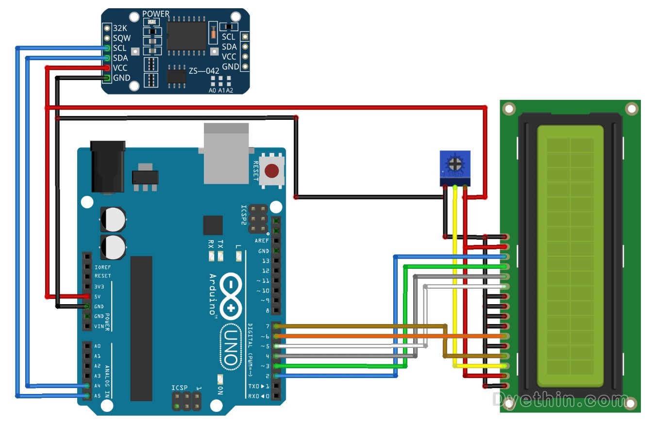
DS3231 RTC Module and Arduino Interface Build Digital Clock and DS3231 Datasheet
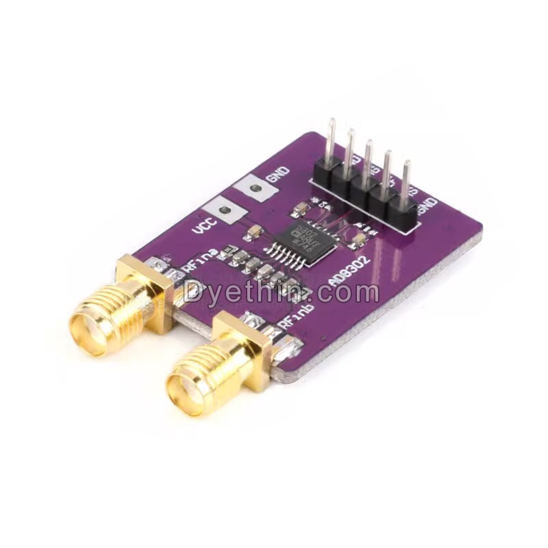
AD8302 signal amplitude phase detection
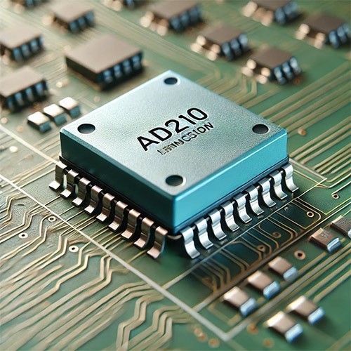
AD210 Precision Isolation Amplifier – Overview and Applications

-

-

-

-

-

-

-

panasonic-electric-works
General Purpose Relays DPST-NO/NC (1 Form A, 1 Form B) 8 A 12VDC
-

-
