


- Startseite
- Featured Products
- Analog Devices
- AD210 Precision Isolation Amplifier – Overview and Applications
AD210 Precision Isolation Amplifier – Overview and Applications
AD210 Introduction
The AD210 is a precision isolation amplifier designed for applications demanding robust signal integrity and electrical isolation. Unlike traditional opto-isolators, the AD210 provides true three-port isolation between input, output, and power supply, making it an ideal choice for industrial measurement and control systems. This compact module operates from a single +15V supply while internally generating isolated ±15V power rails, allowing complete signal and power isolation in a single unit. Engineers across data acquisition and instrumentation sectors rely on the AD210 to eliminate ground loops and prevent signal degradation under harsh operating conditions.
AD210 Features
| Parameter | Specification |
| Isolation Voltage (Continuous) | 2500 Vrms (±3500 V peak) |
| Gain Range | 1 V/V to 100 V/V |
| Gain Nonlinearity (Max) | ±0.012% (B Grade) |
| Gain Temperature Drift | ±25 ppm/°C |
| Bandwidth (Full Power) | 20 kHz (G = 1 V/V), 15 kHz (G = 100) |
| Common-Mode Rejection Ratio | 120 dB (G = 100 V/V) |
| Input Voltage Range | ±10 V (linear), ±15 V (max) |
| Input Impedance (Differential) | 1 MΩ |
| Output Voltage Range | ±10 V (min), load ≥ 2 kΩ |
| Output Impedance | 1 Ω (max) |
| Input Bias Current | 30 pA typ, 400 pA max (@ +25°C) |
| Input Offset Voltage | ±5 mV max (B Grade) |
| Offset Drift (RTI) | ±10 µV/°C ±30/G |
| Isolated Power Output | ±15 V @ 5 mA (input & output) |
| Power Supply | +15 V DC ±5% |
| Quiescent Current | 50 mA |
| Operating Temperature | -25°C to +85°C |
What sets the AD210 apart is its high common-mode voltage (CMV) tolerance of 2500Vrms continuous and ±3500V peak, enabling it to function reliably in high-voltage environments. It supports a wide bandwidth of 20kHz at full power and offers a low gain drift of 25ppm/°C, ensuring consistent performance over temperature fluctuations. With a nonlinearity as low as 0.012%, the AD210 excels in precision measurement. Its isolated power capability—±15V at 5mA on both input and output—further enhances versatility for remote or floating signal sources. Every AD210 module incorporates a flexible input amplifier, allowing custom gain configurations for demanding analog front-end designs.
AD210 Internal Architecture and Signal Flow

AD210 Block Diagram
Inside the AD210, a well-integrated signal path begins with an uncommitted operational amplifier on the input side, providing flexibility for buffering or gain. A full-wave modulator shifts the input signal onto a 50kHz carrier, which is transferred across isolation using transformer coupling. The output stage demodulates the signal and routes it through a low-noise 3-pole filter, finally delivering a buffered, low-impedance output. This signal path ensures that the AD210 offers high-fidelity transmission while rejecting noise and transients common in industrial environments.
AD210 Application Flexibility and Input Configurations

Basic Unity Gain Configuration

Summing or Current Input Configuration
AD210 supports a range of input configurations. It can operate in a unity gain mode or provide programmable gain using external resistors. Whether you're working with small signals that require amplification or designing current-sensing circuits, the AD210's input stage can be configured accordingly. Applications such as summing inputs or handling signals exceeding ±10V are fully supported.

Adjustments for Noninverting Input

Adjustments for Inverting Input
Its non-inverting and inverting adjustment methods offer precision tuning for both gain and offset, allowing seamless integration into custom circuits. These features make the AD210 a go-to component for engineers who demand design flexibility without compromising performance.
AD210 Performance Characteristics
The AD210 offers impressive common-mode rejection ratios (CMRR) up to 120dB when configured for gains of 100 V/V. Its input noise remains extremely low across the bandwidth, maintaining signal clarity in critical applications. Phase shift remains minimal even at higher frequencies, ensuring accurate time-domain signal representation. The amplifier maintains gain accuracy across wide temperature ranges, making the AD210 reliable for both lab and field instrumentation. Engineers appreciate how the AD210 balances speed and precision, especially when working in control loop systems where latency and distortion can lead to instability.
AD210 Built-in Isolated Power Supplies
Each AD210 provides isolated ±15V power on both the input and output sides, simplifying designs that require excitation for sensors or signal conditioning circuits. These supplies support up to 5mA current draw, and their voltage regulation ensures consistent performance under varying loads. With internal bypass capacitors to suppress ripple, the AD210 maintains clean power delivery even under demanding conditions. Short-circuit protection further increases system robustness. For engineers designing fully isolated analog front ends, the AD210 eliminates the need for separate DC-DC converters, reducing BOM and board space.
AD210 Applications

2-Pole, Output Filter
Across various sectors, the AD210 shines in practical applications. In data acquisition systems, it isolates noisy analog signals before digitization, preventing common-mode voltage from corrupting ADC performance. In power monitoring, the AD210 can form a self-powered current source capable of driving a current loop with up to 5mA output. It also serves as a voltage-to-current converter, especially useful for industrial control loops operating over long distances. For thermocouple amplification, the AD210 simplifies cold-junction compensation while preserving signal accuracy. Designers even use AD210 in programmable references, combining it with DACs to create floating precision outputs immune to ground offsets.
AD210 in Multichannel Systems
When used in multichannel systems, the AD210 ensures complete galvanic isolation between channels. Each AD210 can process signals independently without clock synchronization, thanks to its transformer-based modulation scheme. The consistent pinout and slim DIP form factor allow for high-density board layouts. Whether you're building a 4-channel thermocouple reader or a 16-channel data logger, the AD210 simplifies PCB layout while enhancing system safety. Its channel-to-channel noise immunity ensures accurate signal separation even in compact designs, and its built-in power outputs remove the need for separate isolated supplies on each board segment.
AD210 Datasheet
Conclusion
The AD210 delivers a rare combination of precision, isolation, and configurability in a single compact module. Its robust feature set addresses real-world challenges in industrial measurement, automation, and medical instrumentation. The availability of built-in ±15V power, high CMRR, low offset, and flexible input options make it a cornerstone component for engineers building reliable analog front ends. For any design requiring isolation without compromise, the AD210 remains one of the most practical and dependable solutions. With its track record in diverse applications and outstanding electrical characteristics, the AD210 continues to set the benchmark for isolation amplifier performance.
FAQs
Articles you may also like
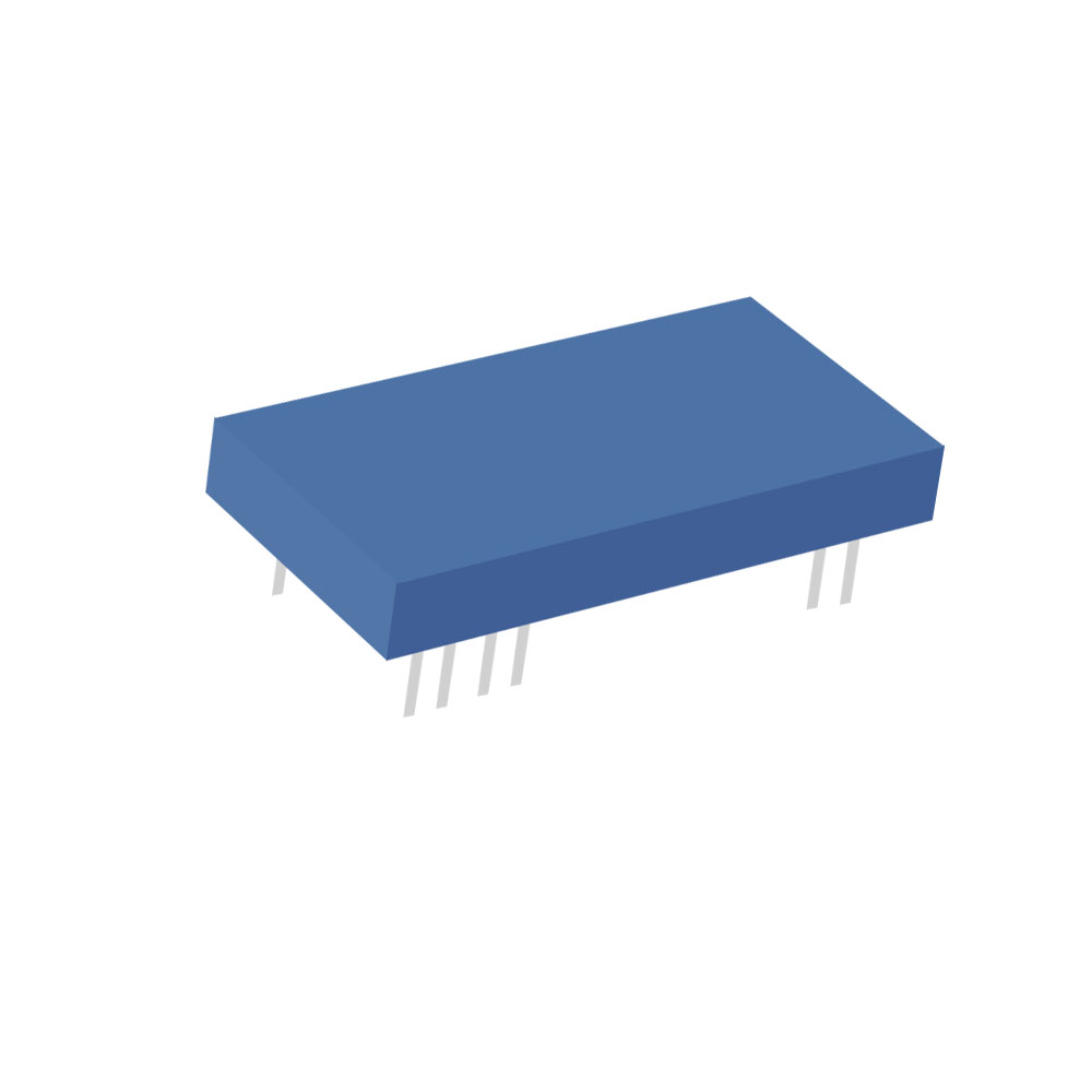
MAX485 is an RS 485/RS422 transceiver integrated circuit IC produced
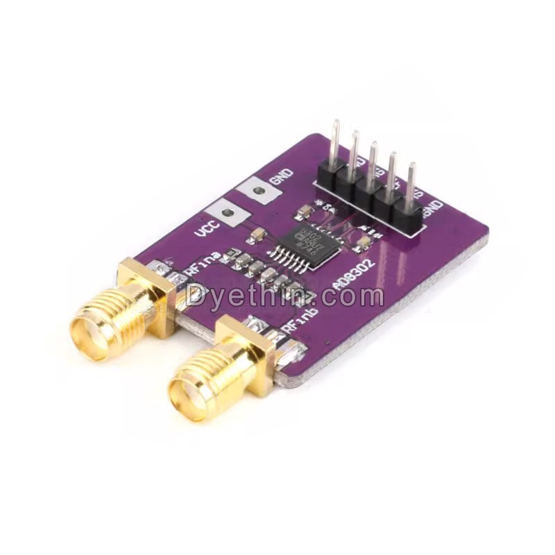
AD8302 signal amplitude phase detection
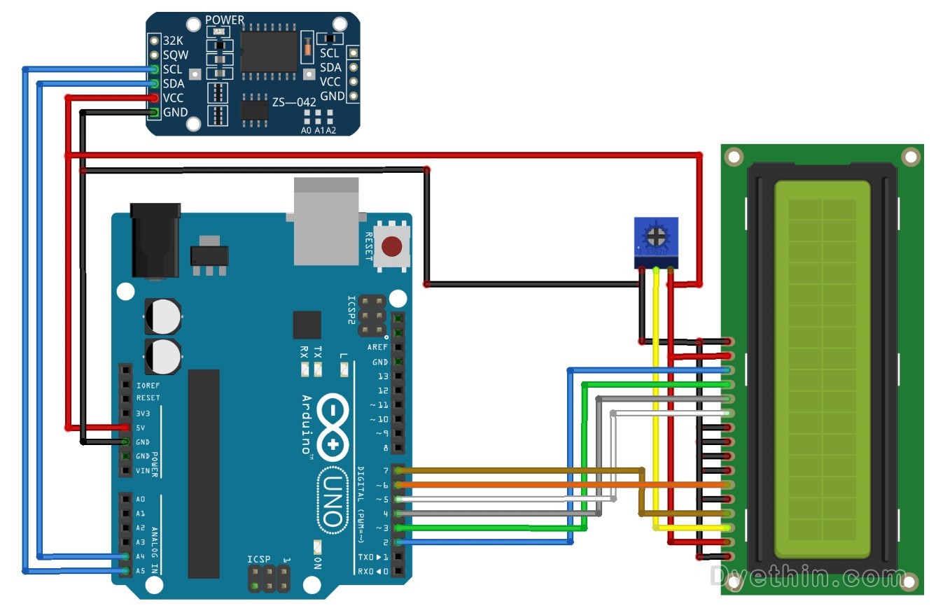
DS3231 RTC Module and Arduino Interface Build Digital Clock and DS3231 Datasheet
Lagerbestand: 10,230


