


Low headroom and minimum load for LDO
[An introduction] In some cases, new multi-gigabit analogue circuits based on deep submicron processes require supply voltages below 1 V. These high-frequency circuits require typically large supply currents, making thermal management challenging. The objective of the design is to reduce power consumption to the minimum level required for circuit performance.
Switching DC-DC converters enhance power supply efficiency, with some devices exceeding 95 percent efficiency, but at the expense of typically wide-bandwidth power supply noise. Low-dropout linear regulators (LDOs) are frequently used to reduce noise in supply rails, but their higher power dissipation increases the system's thermal burden. To mitigate these issues, there is a small voltage difference (headroom voltage) between the input and output voltages when using an LDO. This article's purpose is to examine the impact of limited headroom voltage on power supply rejection and total output noise.
Rejection of LDO Power Supply and Headroom
The LDO power-supply rejection ratio (PSRR) has a strong relationship with the headroom voltage, which is the difference between the input and output voltages. PSRR decreases with increasing load current for a fixed headroom voltage; this is particularly true for large load currents and low headroom voltages. The PSRR of the ADM7160 ultralow noise, 2.5V linear regulator is depicted in Figure 1 at 200 mA load current and 200 mV, 300 mV, 500 mV, and 1 V headroom voltages. As the headroom voltage decreases, the PSRR also decreases, and the dropout voltage can become extremely high. Changing the headroom voltage from 1 V to 500 mV will reduce PSRR by 5 dB at 100 kHz, for instance. However, a small adjustment in the headroom voltage, from 500 mV to 300 mV, decreases the PSRR by greater than 18 dB.

Figure 1: ADM7160 PSRR in relation to headroom.
Figure 2 depicts the LDO block diagram. As the load current increases, the gain of the PMOS pass element will decrease, causing it to exit saturation and enter the three-pole working region. This decreases the overall loop gain and consequently the PSRR. The greater the gain reduction, the lower the surplus voltage. As the headroom voltage continues to decrease, the control loop's gain reaches 1 and the PSRR reaches 0 dB.
The resistance of the pass components, such as the on-resistance of the FET, on-chip interconnect resistance, and bond wire resistance, also reduces loop gain. This resistance can be deduced from the voltage differential. In the WLCSP package, the ADM7160 has a maximum dropout voltage of 200 mV at 200 mA. Using Ohm's law, the pass element's resistance is approximately 1. A fixed resistor and a variable resistor can be used to approximate the adjustment element.
The load current flowing through this resistor reduces the drain-to-source operating voltage of the FET. Using a 1 FET as an example, a load current of 200 mA will cause the drain-source voltage to decrease by 200 mV. When calculating the PSRR of an LDO with 500 mV or 1 V of headroom, the dropout voltage across the pass element must be taken into account because the pass FET operates at only 300 mV or 800 mV.

Figure 2: The block diagram of a low dropout regulator is depicted.
The Influence of Tolerance on the LDO Margin
Customers frequently ask application engineers to help them select an appropriate LDO to generate a low noise voltage X from an input voltage Y when the load current is Z, but the distinction between the input and output voltages is frequently overlooked when setting these parameters. Tolerant behaviour. As the overhead voltage value decreases, the input and output voltage tolerance can significantly impact the operating conditions. Worst-case input and output voltage tolerances always result in a decrease in surplus voltage. In the worst-case scenario, the output voltage may be 1.5% higher and the input voltage may be 3% lower. The worst-case headroom voltage when driving a 3.3 V regulator from a 3.8 V source is 336.5 mV, well below the expected value of 500 mV. The drain-source voltage of the pass FET is only 136.5 mV under a worst-case load current of 200 mA. In this instance, the PSRR of the ADM7160 at 10mA may be significantly lower than the specified 55 dB.
PSRR of LDO when in drop mode
Customers frequently inquire about the PSRR of an LDO in dropout mode to application engineers. This initially appears to be a reasonable query, but the simplified block diagram makes no sense. The output voltage is equal to the input voltage minus the voltage drop caused by the load current of the RDSON of the adjustment FET when the LDO operates in dropout mode. The LDO does not regulate and has no input noise rejection gain; it merely functions as a resistor. The RDSON of the FET forms an RC filter with the output capacitor, which provides a small quantity of residual PSRR; however, a simple resistor or ferrite bead can perform the same function more economically.
Maintain performance in limited headroom operation mode
In the low-headroom mode of operation, the effect of the headroom voltage on the PSRR must be taken into account; otherwise, the output voltage noise level will exceed expectations. As depicted in Figure 3, data sheets frequently include PSRR vs. headroom voltage curves, which can be used to determine the degree of noise rejection feasible under given conditions.

Figure 3: The PSRR versus the headroom voltage.
However, the utility of this information is readily apparent by demonstrating how effectively the PSRR of an LDO filters out noise in the source voltage. When the LDO is operated at various overhead voltages, the total output noise varies as shown in the graph below.
Figure 4 demonstrates the output noise of the 2.5 V ADM7160 with 500 mV headroom and 100 mA load in comparison to the E3631A bench power supply, which is rated for less than 350 V-rms from 20 Hz to 20 MHz. Numerous spurs below 1 kHz are rectification-related harmonics of the 60 Hz line frequency. Large spurs above 10 kHz are caused by the DC-DC converter that generates the ultimate output voltage. Spurs above 1 MHz originate from environmental RF sources unrelated to power supply noise. The power supply utilised for these experiments had a measured noise level of 56 V rms and 104 V-rms, including spurs, over the frequency range of 10 Hz to 100 kHz. The LDO rejects all supply noise with an output noise of approximately 9 V-rms.

Figure 4: Depicts the noise spectral density of the ADM7160 with 500 mV of headroom.
As the headroom voltage falls to 200 mV, noise excursions above 100 kHz begin to intrude into the noise floor as the high frequency PSRR approaches 0 dB. The noise level increases to 10.8 V rms. As the headroom falls to 150 mV, the rectification harmonics begin to affect the output noise, resulting in a 12 V rms increase in output noise. There is a moderate amplitude peak at approximately 250 kHz; therefore, even though the overall noise increase is not significant, sensitive circuits may be negatively impacted. As the headroom voltage decreases, performance degrades and rectification-related spurs appear in the noise spectrum. Figure 5 depicts the output with a surplus of 100 mV. Noise has increased to 12.5 V average. Harmonics contain very little energy, so the increase in spurious noise to 12.7 V rms is minimal.

Figure 5: Depicts the noise spectral density of the ADM7160 with 100 mV of headroom.
With a headroom of 75 mV, output noise is severely degraded, as rectified harmonics appear across the spectrum. Rms noise reaches 18 V rms, while noise plus spurs reaches 27 V rms. Noise above 200 kHz is attenuated because the LDO loop has no gain and functions as a passive RC filter. The ADM7160 operates in dropout mode when the headroom reaches 65 mV. As shown in Figure 6, the ADM7160's output voltage noise is practically identical to its input noise. The rms noise is 53 V and the rms noise plus spurs is 109 V. Noise above 100 kHz is attenuated because the LDO functions as a passive RC filter.

Figure 6: Noise spectral density of the ADM7160 in dropout mode, as shown.
Superior PSRR and Ultralow Noise LDO
Modern LDOs, such as the ADM7150 ultralow noise, high PSRR regulator, cascade two LDOs so that the PSRR is roughly equal to the aggregate of the PSRRs of the single-stage LDOs. These LDOs have a PSRR greater than 60 dB at 1 MHz and well greater than 100 dB at lower frequencies, but require slightly higher clearance voltages.
Figure 7 depicts the noise spectral density of the 5 V ADM7150 with a 500 mA load current and an 800 mV leeway. The output noise from 10 Hz to 100 kHz is 2,2 V rms. As the headroom decreases to 600 mV, rectification harmonics begin to appear and the output noise increases to 2.3 V rms, which contributes minimally to the noise.

Figure 7: Depicts the noise spectral density of the ADM7150 with a headroom of 800 mV.
As depicted in Figure 8, when the headroom is 500 mV, the rectified harmonics and the 12 kHz peak are plainly visible. The noise of the output voltage increases to 3.9 V rms.

Figure 8: Depicts the noise spectral density of the ADM7150 with 500 mV of headroom.
When the available headroom is 350 mV, the LDO enters dropout mode. As depicted in Figure 9, the LDO can no longer modulate the output voltage, acting as a resistor, and the output noise increases to nearly 76 V rms. Only the pole formed by the RDSON of the FET and the capacitance at the output attenuate input noise.

Figure 9: Depicts the ADM7150's noise spectral density in dropout mode.
To conclude
Modern LDOs are increasingly used to reduce noise in supply rails, which are typically implemented with switching regulators that generate noise across a broad frequency range. Switching regulators generate these voltage gradients with high efficiency, whereas power-hungry LDOs reduce noise and reduce efficiency simultaneously. Consequently, the LDO's operating headroom voltage should be as low as feasible.
As stated previously, the PSRR of the LDO is a function of the load current and the headroom voltage, and it will decrease as the load current or headroom voltage increases. This is because the loop gain will decrease when the operating point of the regulator tube moves from the saturated work area to the three-pole work area.
Taking into account input source noise characteristics, PSRR, and worst-case tolerance, designers can simultaneously optimise power consumption and output noise for sensitive analogue circuits.
With extremely low headroom voltages, the worst-case input and output voltage tolerances can have an effect on PSRR. A robust design can be achieved by considering the worst-case tolerance; otherwise, the resulting power solution will have a lower PSRR and higher total noise than anticipated.
Articles you may also like
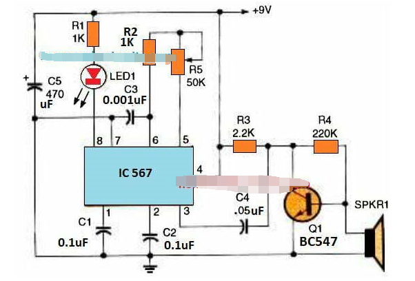
Simple and Useful Ultrasonic Transmitter and Receiver Circuit
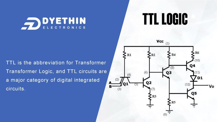
The working principle and usage method of TTL circuit
How to design an overvoltage protection circuit?
Automotive taillight control circuit design

-

-

-

-

-

-

-

-

-

omron-electronics-inc-emc-div
General Purpose Relays DPST-NO (2 Form A) 5 A 12VDC