


Automotive taillight control circuit design
Design objective
Create a circuit capable of controlling automobile taillights by repurposing ternary counters and decoders, as well as display driver and switch control circuits. This circuit employs light-emitting diodes to simulate taillights in order to simulate four driving situations: normal driving, a right turn, a left turn, and emergency braking.
Design specifications
Assume there are three signal lamps on the left and right sides of the car's rear (simulated with luminescent tubes):
(1) During normal travel, all tail lights are turned off;
(2) When the vehicle turns right, the three right-side indicators illuminate in the correct order.
(3) When the vehicle turns left, the three left indicators illuminate sequentially.
(4) When the car is under emergency braking, all indicators flash at the same moment;
(5) Be an expert in the design, simulation, and debugging of taillight control circuits for automobiles;
(6) Design circuit diagrams, simulate, analyze, and summarize simulation results using the appropriate software.
Operating principle and block diagram of vehicle taillight control circuit
A switch control circuit, a multivibrator circuit comprised of a 555 timer, an LED display, a drive circuit, a decoder, and a ternary counter constitute the automobile taillight control circuit. A 74LS112 chip is used to connect the circuit in order to create a ternary counter, while a 74LS138 chip, six NAND gates, and six inverters are utilized to create a decoding circuit. The design creates a circuit that regulates the car's six taillights (three on each side). Use two toggle switches as turn signal sources, one exclusively for right turns and the other for left turns. If both switches are activated, an emergency deceleration situation is indicated and the emergency flasher illuminates. When turning, all of the tail lights on one side are illuminated and all of the tail lights on the opposite side are off, with the illuminated lights flashing intermittently every second. When the emergency flashers are activated, the six rear lights flash at a rate of 1 Hz.

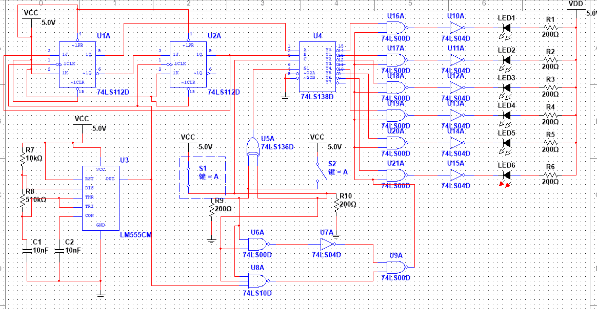
Car taillight control circuit schematic block diagram
Circuit design and simulation for each unit
1 Indicator
1.1 Construct a circuit diagram

Circuit diagram for oscillator design
1.2 Description and simulation of the design
The oscillator is this circuit's central component. The oscillator's stability has a direct impact on the operation of the decoder and switch control circuit and an indirect impact on the final blinking frequency of the car's taillights. This design employs a multivibrator comprised of a 555 timer and a programmable RC, which influences the clock pulse CP terminals of two 74LS112D and an input terminal of the 74LS10D.

The image above depicts the oscillator's simulation waveform diagram and frequency test. As depicted, the oscillator is capable of producing a standard square wave.

Oscillator testing graphs
2 Control circuit for a
2.1 Construct a circuit diagram

switch control schematic
2.2 Description and simulation of the design
1.U1A XOR logic U1A outputs 1 when S0 and S1 are different, i.e., when the vehicle is turning left or right, and 0 in all other states (normal operation or emergency deceleration). U1A outputs to the G1 terminal of the 74LS138D circuit, and the G1 terminal is under the control of U2. The chip is on and off because it only functions when it needs to turn left and right; therefore, only when the output of U1A is 1 does the chip function and produce cyclic signals.
The output signal of S0 is also transmitted to the input of the 74LS138D chip in order to determine whether the vehicle will turn left or right. When S0 equals 1 and S0 differs from S1 (UA1 outputs 1), the sign turns to the right, the chip functions, and the cycle signal causes D4 D5 D6 (the last three lights) to flash in a cycle.
When S0 = 0 and S0 is different from S1 (UA1 outputs 1), the sign turns left, the chip functions, and the generated cyclic signal causes D1 D2 D3 (the first three lights) to blink cyclically.
2.U2A NAND logic circuit When s0 and s1 are both closed, the device passes through the NOT gate U3A and the output is 1.
When either s0 or s1 is disconnected, the device passes through the NOT gate and produces a 0 output.
3. The input of U4A is analogous to that of U2A, with the addition of a square wave input from a multivibrator.
4. U5A outputs to the light control, primarily functions during braking, and outputs a rectangular wave during emergency braking.
This is the corresponding truth table:
| S0 S1 multi-association | U1A | U3A | U4A | U5A | meaning |
| 0 0 * | 0 | 0 | 1 | 1 | The car is running normally, and all 6 lights of the control are off |
| 0 1 * | 1 | 0 | 1 | 1 | Turn left, U1A=1, indicating that S0 and S1 are different, S0 is input to 74LS138D, the sign is not a right turn, but a left turn |
| 1 0 * | 1 | 0 | 1 | 1 | Right turn, s0 input to 74LS138D sign turn right |
| 1 1 1 | 0 | 1 | 0 | 1 | Emergency brake. At this moment, the square wave is 1 and all 6 lights are off. |
| 1 1 0 | 0 | 1 | 1 | 0 | Emergency brake: The square wave is 0 at this moment, and all 6 lights are on. |
When the emergency blinkers are activated, the six taillights flicker on and off in unison at a rate of approximately one hertz (Hz).
1. emergency braking system
Realize the effect when the six LEDs flash on and off in unison at a rate of approximately 1 hertz.
Status: U1A output is zero, the 74LS138D chip is defective, and each port emits one.
1.1 When the U5A output is 0, the NAND gate and NOT gate turn on all six taillights D1 D2 D3 D4 D5 D6.

D1 D2 D3 D4 D5 D6 with maximum luminance

D1 D3 input waveform diagram for the front-end
In the experiment, it was determined that a minor error occurred when all six lights flashed simultaneously. The flashing was not precisely synchronized, but the waveform output (D1D3 output in the image) was nearly so.
1.2 When UA5=1, the output of Y0 Y1 Y2 Y3 Y4 and Y5 is 1.

No lights are on
2.When turning right, s0 equals 1, UA1 outputs 1, and 74LS138D output pins Y3, Y4, and Y5 are successively low, causing D4, D5, and D6 to illuminate sequentially.

Right turn switch control diagram
1.When turning left, 74LS138D output pins Y0, Y1, and Y2 are each at a low level, causing D1, D2, and D3 to turn on in sequence.

switch status control
3 LED display and power supply
3.1 Construct circuit schematic

schematic of LED display and drive circuit
3.2 Design guidelines
74LS138, six NAND gates, and six inverters compose the decoding circuit.
The three input terminals C, B, and A of 74LS138 are respectively connected to S0, Q1, and Q0. When S1 = 1, S0 = 0, and the enabling terminal signal A=G = 1, the state of the counter is 00, 01, 10, and the output terminals Y0, Y1, and Y2 of the decoder are sequentially active at a low level. The NOT gate causes the indicator lamps D1D2D3 connected to R3, R4, and R5 to illuminate sequentially to indicate that the vehicle will turn left. Similarly, when S1=0 and S0=0, the indicator lights D4D5D6 will illuminate in a cyclical sequence to indicate a right turn. When G=0 and A=1, the output terminals of 74LS138 are all 1 (high level), and the indicator lights are off, indicating that the vehicle is operating normally. And when G = 0 and A = CP, all indicator lights will blink cyclically at the rate of CP to indicate that the vehicle should brake in an emergency.
4 Ternary opposition
4.1 Construct a circuit diagram

Ternary counter structure
4.2 Design guidelines
A ternary counter is utilized, and the count consists of the three digits 00, 01, and 10. Consequently, only two JK flip-flops are required, and the 11 state is not implemented. We chose to use two 74LS112Ds as a result. Connect the two JK flip-flops to a synchronous addition counter (quaternary) inside the microprocessor before converting it to a ternary system. When the counter reaches 3, the output state will be 11. The state 11 is used to generate a reset signal to reset the two flip-flops to their initial state of 0. Then the number three will not be displayed. Maximum value is 2, which corresponds to the required ternary counter.
Detailed explanation of combinational logic circuit
1 Multivibrator circuit
Multivibrator is also known as an astable flip-flop because it has no stable output state and only two stable transient states. After a period of time in a particular transiently stable state, the circuit can reverse to another transiently stable state on its own. By converting the two transient states to each other, a series of rectangular waves is generated.
The oscillation frequency of the 555-timer-based multivibrator is stable and not readily perturbed. In addition, the design of the control circuit does not necessitate a high level of pulse precision so long as it is adjustable. As a result, in the circuit design of this device, a 555 timer-based multivibrator was selected as a pulse generator.

555 timer pinout schematic

555 timer diagram of functions
2 Decoder
74LS138 is a three-to-eight-line decoder. With three variable inputs and a 3-line to 8-line decoder, the 74LS138 can form any logic function. A 3-line to 8-line decoder can be used for any logic function with three input variables. The 74LS138 decoder is implemented. Because any combinatorial logic expression can be written as a standard AND or expression, that is, as the sum of the minterms, and the output of the block 3-line-8-line decoder 74LS138 is the exact full expression of the two-variable minterm.

74LS138 pinout schematic

74LS138 table of functions
3 Ternary opposition
The counter calculates the accumulation of time and outputs it in 8421BCD code. To display the 8421BCD code emitted by the counter, a decoding display circuit is required to convert the digital output of the counter into the output logic and a specific current required by the digital display device. Consequently, we employ a common cathode seven-segment digital display tube and 74LS48 as a decoder; Among them, the pin diagram and function table of 74LS48 are shown in Figure 8 and Figure 9.

Ternary counter 74LS112 chip pin diagram
| pin number | Function Description |
| 1(CLK1)、13(CLK2) | Clock input (falling edge valid) |
| 2(K1)、3(J1)、13(K2)、14(J2) | data input |
| 5 (Q1), 6 (Q1 not), 7 (Q2 not), 9 (Q2) | output |
| 14(CLR1)、15(CLR2) | Direct reset terminal (active low) |
| PR1、PR2 | Directly set terminal (active low) |
Ternary counter 74LS112 chip pin explanation

74LS112 Function Table
Test of combined function
The entire circuit is capable of performing four functions: left turn, right turn, normal travel, and emergency braking.

General circuit diagram
1 Left turn capability
When both S1 and S2 are accessible. At this point, the vehicle enters the left turn state, and D1D2D3 illuminates cyclically.
")
")
")
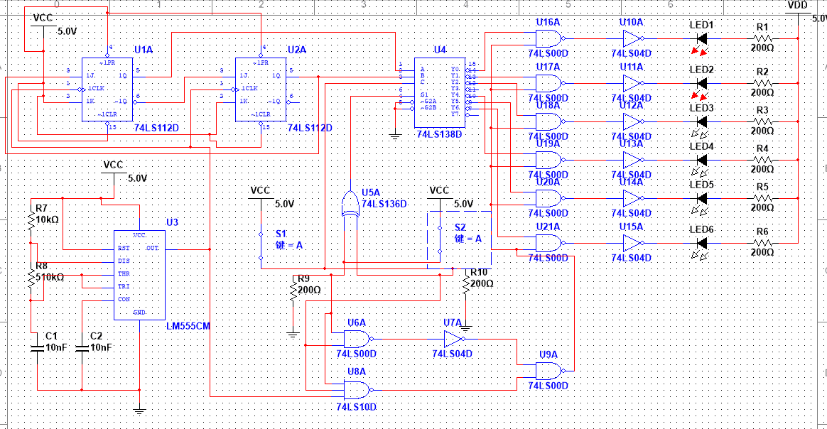
Left turn test (D1D2D3 cycle light)
2 Right turn capability
When S2 is open and S1 is closed. At this juncture, the right turn state must be entered. D4D5D6 illuminates sequentially.
")
")
")
Right turn test (D4D5D6 cycle light)
3 Standard driving
When S1 is severed, S2 is severed as well. Currently, the vehicle is in a normal operating condition, and all LED lights are off.
")
Normal driving (all lights off)
4 Emergency stopping capability
When S1 is closed, so too is S2. Currently, it is in emergency braking mode, with all LED indicators flashing.
")
Emergency brake test (LED flashes at the same time)
Summarize
This experiment demonstrated the control of automobile taillights. The experiment must be controlled using a ternary counter and decoder.
Two 74LS112 chips implement ternary counters that continually count from 0 to 2 (decimal). The results of the two counters are input to the A and B ends of the 74LS180D decoder and are controlled by the closure and opening of S0 74LS180D chip input selection A or B. ① When A is selected, the decoder receives the 0-2 cyclic input of the A port, causing Y0, Y1, and Y2 to be at low levels in sequence, thereby controlling the cyclic blinking of D1, D2, and D3. ② When B is selected, the decoder can receive the 0-2 cyclic input of the B port, lowering Y3, Y4, and Y5 sequentially to control the cyclical blinking of D3, D4, and D5.
In the experiment, the multivibrator was primarily used to generate rectangular waves, and the six tail lights flickered with a frequency of approximately 1Hz.
Sample GIF:
Make a left:

Make a right:
emergency stop:
Articles you may also like
Simple and Useful Ultrasonic Transmitter and Receiver Circuit
The working principle and usage method of TTL circuit

How to design an overvoltage protection circuit?
Interpret the 1N4007 Datasheet to understand what Schottky diode are

-

-

-

-

-

-

-

-

-

rainsun-corporation