













- Accueil
- Blogs
- Power management
- Principles and applications of LDO
Principles and applications of LDO
LDO definition
LDO, lowdropoutregulator, is a low dropout linear voltage regulator. This is compared to traditional linear regulators. Traditional linear voltage regulators, such as the 78XX series of chips, require the input voltage to be at least 2V~3V higher than the output voltage, otherwise they will not work properly. But in some cases, such conditions are obviously too harsh. For example, when converting 5V to 3.3V, the voltage difference between the input and output is only 1.7v, which obviously does not meet the working conditions of traditional linear regulators. In response to this situation, chip manufacturers have developed LDO voltage conversion chips.
Characteristics of LDO
Low dropout (LDO) linear regulators have low cost, low noise, and small quiescent current, which are their outstanding advantages. It also requires very few external components, usually only one or two bypass capacitors. The new LDO linear regulator can achieve the following specifications: output noise of 30μV, PSRR of 60dB, quiescent current of 6μA, and voltage drop of only 100mV.
After reading the above definition, without understanding the LDO structure, everyone can think of the low-voltage drop regulator in the figure below using analog electrical knowledge.
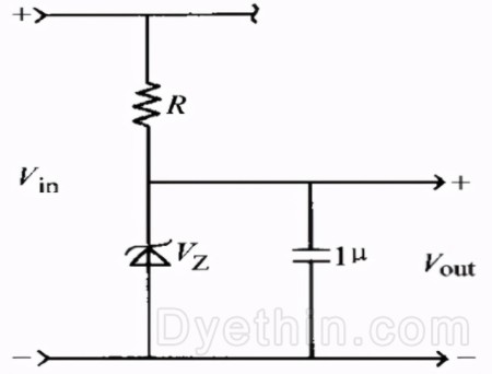
The picture above is the most basic voltage stabilizing circuit. The core component is the voltage stabilizing tube. Its voltage stabilizing working range determines the output voltage stabilizing range. Through this simple circuit, small current (hundred mA level) and small dynamic range can be achieved. internal voltage stabilization.
Upgrade the above circuit as shown below:
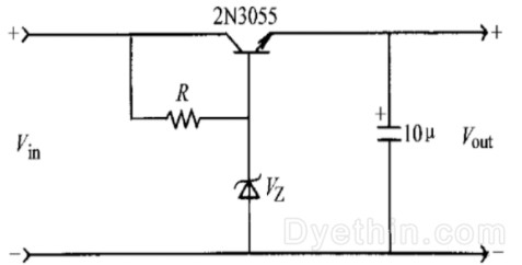
The above circuit only has one more 2N3055 transistor, which is intended to improve the output load capacity. At the same time, the transistor also introduces voltage negative feedback to stabilize the output voltage. When the input voltage Vin increases or the output load resistance increases, the output voltage Vout will increase instantaneously, and the emitter voltage Ve of the transistor will increase accordingly. If the base voltage Vb remains unchanged, Vb-Ve will decrease, and then The output current decreases and Vout decreases.
The picture above is just a simple and basic low-dropout voltage regulator. Note that there is a difference between the word "linear" and the LDO we are talking about. It can be seen here that the output voltage Vout of the above circuit will be affected by the fluctuation of Vbe voltage and has poor stability. And the output voltage cannot be adjusted.
LDO circuit
On the basis of the above circuit, a "linear" factor is added, that is, an operational amplifier is introduced to deepen the negative feedback and improve the stability of the output voltage. This also constitutes what we call a low dropout linear regulator. The circuit diagram is as follows
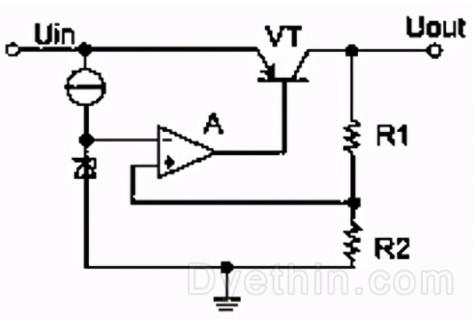
On the basis of the basic voltage regulator tube adjustment circuit, an operational amplifier A and a voltage dividing resistor sampling network R1 and R2 are added. When the input voltage Vin increases or the output load resistance increases, the output voltage Vout will increase instantaneously, and the voltage obtained through voltage division sampling by R1 and R2 will also increase. Since it is the reverse terminal input, the output of op amp A will decrease accordingly. Then Vb-Ve will decrease, then the output current will decrease, and Vout will decrease. As can be seen from the circuit in the above figure, LDO divides the voltage through resistors, that is, LDO can only step down the voltage, not boost it. And the current cannot be too large.
LDO application
There are many kinds of LDO chips. The ones I have used include AMS1117, SPX3819, TLV702x, etc. Let's take SPX3819 as an example to briefly talk about the application of LDO.
The features of SPX3819 are as follows
(1) Low noise: may reach 40uV
(2) High accuracy: 1%
(3) Battery reverse connection protection
(4) Low voltage drop: 340mV at full load
(5) Low quiescent current: 90uA
(6) Zero off-mode current
(7) Fixed output: 1.2V, 1.5V, 1.8V, 2.5V, 3.0V, 3.3V, 5.0V
Different LDOs have different performances, and everyone chooses them according to their actual project needs.
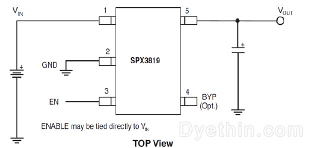
The circuit diagram of spx3819 is as follows. You can see that the LDO peripheral circuit is very simple. This is also the advantage of LDO.
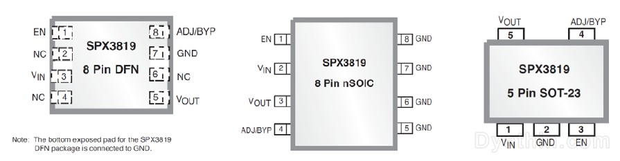
SPX3819 provides 3 different packages, suitable for many scenarios.
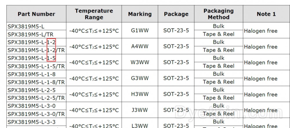
It has an output rated voltage version, which is the fixed output mentioned above: 1.2V, 1.5V, 1.8V, 2.5V, 3.0V, 3.3V, 5.0V, distinguished by different model suffixes.
Of course, a voltage-regulated version is also provided. The circuit and output voltage formula are as follows

Power consumption problem
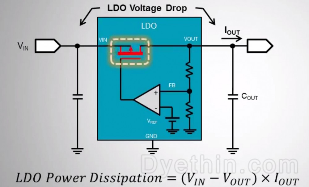
We explained above that the principle of LDO is to divide the voltage through resistors, which makes LDO not suitable for high current scenarios, generally not more than 1A. This also brings up topics that LDO cannot avoid: power consumption and heat dissipation issues.
The first thing to consider when choosing an LDO is the maximum input voltage range of the LDO and the LDO current output capability.
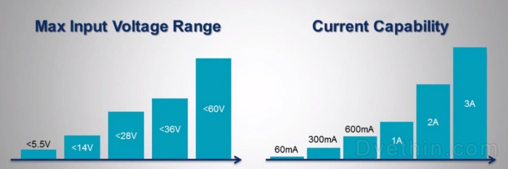
Then larger current or larger LDO voltage drop will result in higher component power loss
The graph below shows the relationship between LDO voltage drop and LDO current at a specific power
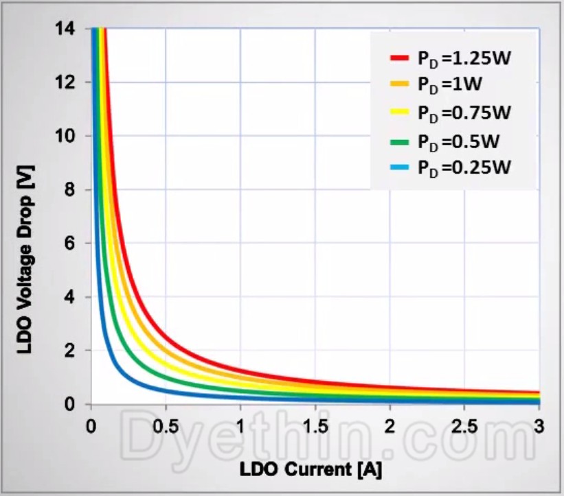
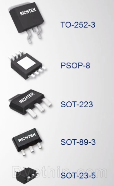
When the power consumption of LDO increases, the heat dissipation function of the LDO package must also be able to match. Common packages are as follows
The power consumption of an LDO is determined by multiplying the voltage drop across the LDO by the current flowing through the LDO. The power is mainly lost in the conductive components of the LDO, which causes the silicon crystal to heat up.
The power lost depends on the IC package, PCB layout, and ambient temperature
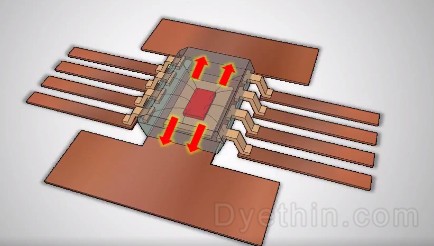
For example: SOT23 package, the perspective view is as follows
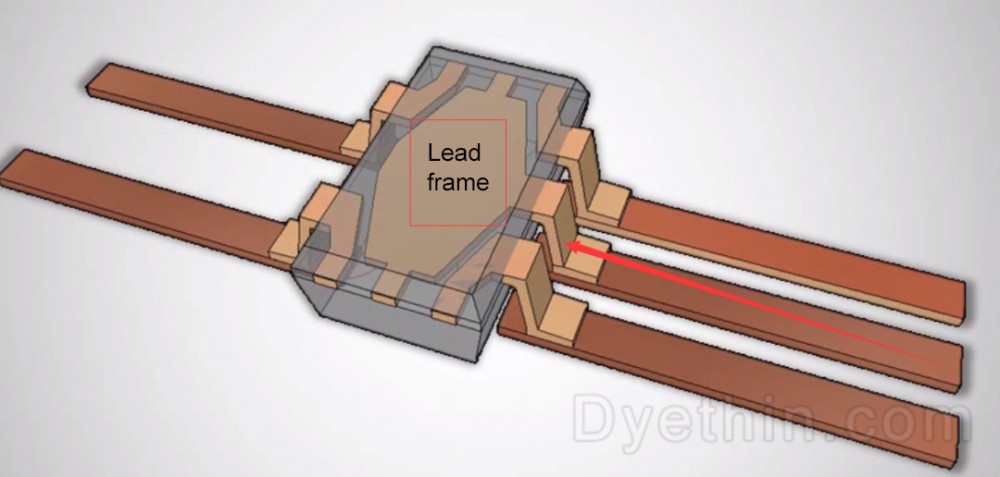
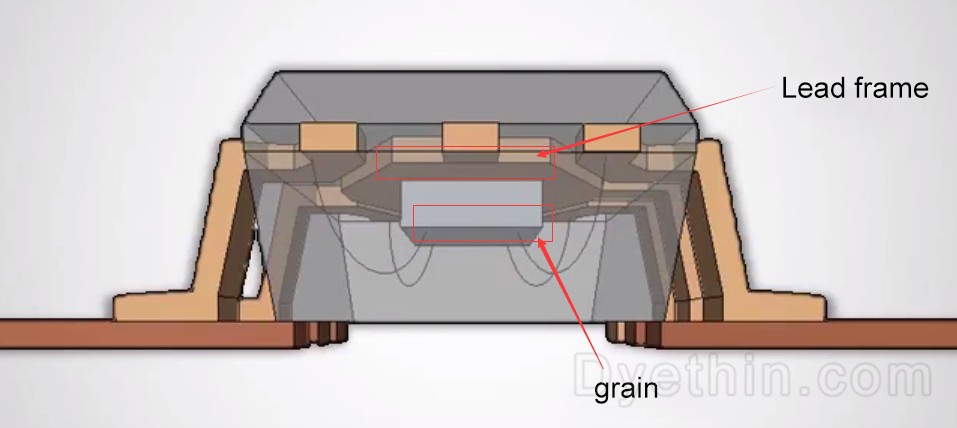
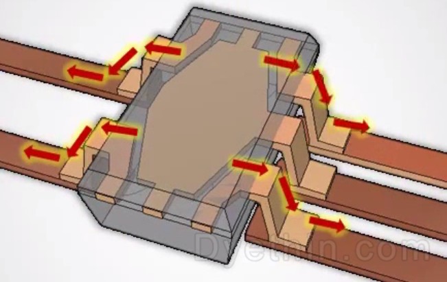
The center pin connects to the leadframe attached to the die. The heat dissipation is mainly to dissipate heat into the air and to the PCB through the pins.
Because the bonding line between the outer pins and the silicon grain is very thin, that is, the 4 pins in the picture below, heat dissipation is mainly based on the middle pins. As mentioned above, the middle pins are connected to the lead frame. Therefore, the PCB with the middle pin can be designed to be wider.
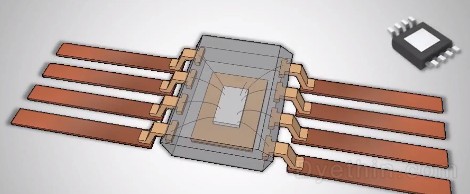
There is also an SOP-08 package, and the bottom copper wire can also be used for heat dissipation.
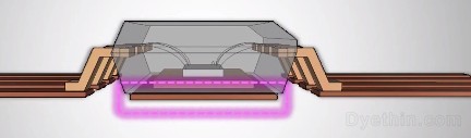
If designed according to the figure below, the heat dissipation effect will be better
Understanding Low Dropout Regulators (LDOs)
Low-dropout regulators (LDOs) may seem simple, but they can provide important functions, such as isolating loads from dirty supplies or building low-noise power supplies to power sensitive circuits.
This short tutorial introduces some commonly used LDO related terminology, as well as some basic concepts such as dropout voltage, headroom voltage, quiescent current, ground current, shutdown current, efficiency, DC input voltage and load regulation, input voltage and load instantaneous response, power supply rejection ratio (PSRR), output noise, and accuracy. At the same time, in order to facilitate understanding, examples and illustrations are used in the text.
LDO selection is usually not done until late in the design process, and analysis is rarely performed. The concepts described in this article will enable designers to select the best LDO based on system requirements.
pressure difference
Dropout voltage (VDROPOUT) is the input-to-output voltage difference when the input voltage drops further enough that the LDO can no longer regulate. In the dropout region, the trim element acts like a resistor with a value equal to the drain-to-source on-resistance (RDSON). The voltage difference is expressed as RDSON and load current as:
VDROPOUT = ILOAD × RDSON
RDSON includes the pass element resistance, on-chip interconnect resistance, pin resistance and wire bond resistance, and can be estimated from the LDO voltage drop. For example, in the WLCSP package, the ADP151 has a worst-case dropout voltage of 200 mW at a 200 mA load, so the RDSON is approximately 1.0 Ω. Figure 1 shows the schematic diagram of the LDO. In dropout mode, the variable resistance is close to zero. LDOs cannot regulate the output voltage, so input voltage and other parameters such as load regulation, accuracy, PSRR, and noise are meaningless.
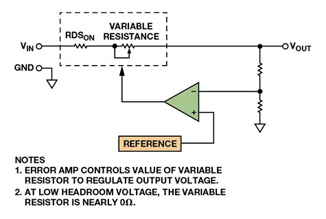
Schematic diagram of LDO
The picture below shows the relationship between the output voltage and the input voltage of the 3.0V ADM7172 LDO. The dropout voltage at 2 A is typically 172 mW, so RDSON is approximately 86 mΩ. The dropout region drops from an input voltage of approximately 3.172 V to 2.3 V. Below 2.3 V, the device does not operate properly. The dropout voltage drops proportionally with smaller load currents: at 1 A, the dropout voltage is 86 mV. Low differential pressure maximizes regulator efficiency.
3.0 The relationship between the output voltage and input voltage of 3.0V ADM7172 LDO
Headroom voltage
Headroom voltage is the input-to-output voltage difference required by the LDO to meet its specifications. Data sheets often refer to headroom voltage as a condition against which other parameters are specified. Headroom voltage is typically about 400 mV to 500 mV, but some LDOs require headroom voltages as high as 1.5 V. Headroom voltage should not be confused with dropout voltage as the two are the same only when the LDO is operating in dropout mode.
Quiescent current and ground current
Quiescent current (IQ) is the current required to power the LDO's internal circuitry when the external load current is zero. It includes the operating current of the bandgap reference voltage source, error amplifier, output voltage divider, and circuits such as overcurrent and overtemperature detection. Quiescent current is determined by topology, input voltage, and temperature.
IQ = IIN (no load)
When the input voltage changes between 2 V and 5.5 V, the quiescent current of the ADP160 LDO is almost constant, as shown in the figure below
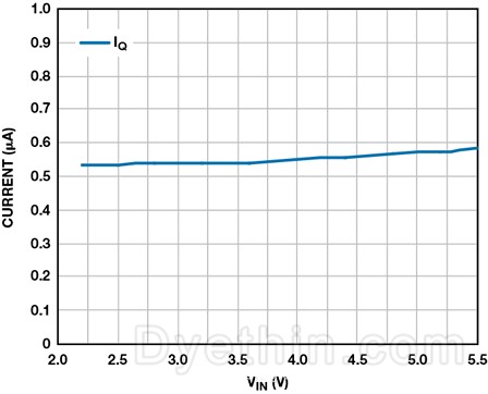
ADP160 LDO Quiescent Current vs. Input Voltage
Ground current (IGND) is the difference between input current and output current, and must include quiescent current. Low ground current maximizes LDO efficiency.
Ignd= Iin– Iout
The picture below shows the change in ground current versus load current for the ADP160 LDO.
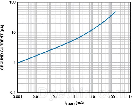
ADP160 LDO Ground Current Change vs. Load Current
For high-performance CMOS LDOs, the ground current is typically much less than 1% of the load current. Ground current increases with load current because the gate drive of the PMOS pass element must increase to compensate for the voltage drop caused by its RON. In the dropout region, the ground current also increases as the driver stage begins to saturate. CMOS LDOs are critical for applications requiring low power consumption or small bias current.
Shutdown current
Shutdown current is the input current consumed by the LDO when the output is disabled. Neither the reference circuit nor the error amplifier is powered up in shutdown mode. Higher leakage current causes the shutdown current to increase with temperature, as shown in the figure below.
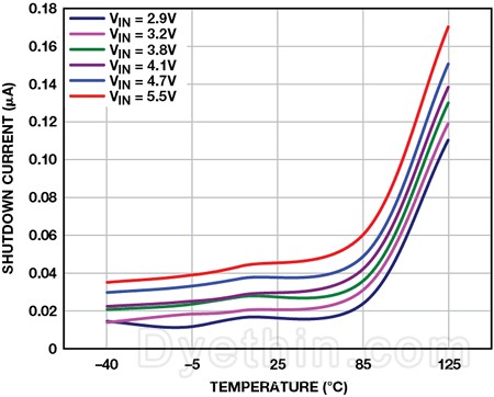
ADP160 LDO Shutdown Current vs. Temperature
Efficiency
The efficiency of an LDO is determined by ground current and input/output voltage:
Efficiency = IOUT/(IOUT + IGND) × VOUT/VIN × 100%
To achieve high efficiency, headroom voltage and ground current must be minimized. Additionally, the voltage difference between input and output must be minimized. The input-to-output voltage difference is intrinsic to determining efficiency, regardless of load conditions. For example, when operating from a 5 V supply, the efficiency of a 3.3 V LDO never exceeds 66%, but when the input voltage is reduced to 3.6 V, its efficiency increases to a maximum of 91.7%. The power consumption of the LDO is (VIN – VOUT) × IOUT.
DC load regulation
Load regulation is a measure of the LDO's ability to maintain the rated output voltage when load conditions change. The load regulation rate is defined as follows (As shown below):
Load regulation = ΔVOUT/ΔIOUT

Relationship between ADM7172 LDO output voltage and load current
DC input voltage regulation rate
Input voltage regulation is a measure of the LDO's ability to maintain the specified output voltage when the input voltage changes. Input voltage regulation is defined as:
Input voltage regulation = ΔVOUT/ΔVIN
The picture below shows the relationship between the output voltage and the input voltage of the ADM7172 under different load current conditions. Input voltage regulation worsens as load current increases because the LDO's total loop gain decreases. In addition, the power dissipation of the LDO also increases with the input-to-output voltage difference, which causes the junction temperature to increase and the bandgap voltage and internal offset voltage to decrease.
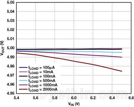
Relationship between ADM7172 LDO output voltage and input voltage
DC accuracy
Overall accuracy takes into account the effects of input voltage and load regulation, reference voltage drift, and error amplifier voltage drift. Changes in the output voltage on a regulated power supply are mainly caused by temperature changes in the reference voltage source and error amplifier. If discrete resistors are used to set the output voltage, the tolerances of these resistors may be the largest factor affecting overall accuracy. The impact of input voltage and load regulation and error amplifier offset on overall accuracy is typically 1% to 3%.
For example, the following operating characteristics can be used to calculate the overall accuracy of a 3.3 V LDO over the 0°C to 125°C temperature range: resistor temperature coefficient of ±100 ppm/°C, sampling resistor tolerance of ±0.25% due to load adjustment The output voltage changes caused by input voltage adjustment are ±10 mV and ±5 mV respectively, and the accuracy of the reference voltage source is 1%.
Error due to temperature = 125°C × ±100 ppm/°C = ±1.25%
Error due to sampling resistor = ±0.25%
Error due to load regulation = 100% × (±0.01 V/3.3 V) = ±0.303%
Error due to input voltage regulation = 100% × (±0.005 V/3.3 V) = ±0.152%
Error due to voltage reference = ±1%
Worst-case errors assume that all errors vary in the same direction.
Worst case error = ±(1.25% + 0.25% + 0.303% + 0.152% + 1%) = ±2.955%
Typical error assumes random variation, so the root square root (rss) of this error is taken.
Typical error = ±√(1.252 + 0.252 + 0.3032 + 0.1522 + 12) = ±1.655%
The LDO never exceeds the worst case error, and the rss error is the most likely error. The error distribution will be centered around the rss error and expanded to include the worst-case error in the tail.
Load transient response
Load transient response refers to the change in output voltage when the load current changes stepwise. It is related to the value of the output capacitor, the equivalent series resistance (ESR) of the capacitor, the gain bandwidth of the LDO control loop, and the magnitude and rate of load current change.
The rate of change of the load transient can have a significant impact on the load transient response. If the load transient is very slow, say 100 mA/μs, the LDO's control loop may be able to track the change. However, if the load transient is fast and the loop is unable to compensate, erratic behavior may occur, such as excessive ringing due to low phase margin.
The image below shows the response of the ADM7172 to a 1 mA to 1.5 A load transient at a slew rate of 3.75 A/μs. A 0.1% recovery time of 1.5 μs and minimal ringing indicate good phase margin.
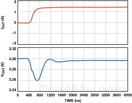
ADM7172 load transient response. A load step of 1 mA to 1.5 A occurs in 400 ns (red line). Output voltage (blue line)
Line transient response
Input voltage transient response refers to the change in output voltage when the input voltage changes stepwise. It is related to the gain bandwidth of the LDO control loop and the magnitude and rate of input voltage change.
The picture below shows the response of the ADM7150 to a 2 V input voltage step change. The output voltage deviation also characterizes the loop bandwidth and PSRR (see next section). Corresponding to a 2 V change in 1.5 μs, the output voltage changes by approximately 2 mV, indicating a PSRR of approximately 60 dB at approximately 100 kHz.
Likewise, as in load transients, the rate of change of the input voltage also has a greater impact on the input transient response. Ringing or other unusual behavior can be hidden when the input voltage changes slowly (just a dip in the LDO's bandwidth).
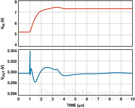
ADM7150 line transient response. A line step from 5 V to 7 V occurs in 1.5 μs (red line). Output voltage (blue line)
Power supply suppression
Simply put, PSRR is a measure of how well a circuit suppresses extraneous signals (noise and ripple) that appear at the power input so that these interfering signals do not destroy the performance of the circuit's output. PSRR is defined as:
PSRR = 20 × log(VEIN/VEOUT)
Among them, VEIN and VEOUTT are the external signals appearing at the input end and output end respectively.
For circuits such as ADCs, DACs, and amplifiers, PSRR applies to the inputs that power the internal circuitry. For LDOs, the input power pin supplies both the internal circuitry and the output voltage. PSRR has the same relationship as DC input voltage regulation, but includes the entire frequency spectrum.
Power supply rejection in the 100 kHz to 1 MHz range is important because LDOs are often used with high-efficiency switching power supplies to power sensitive analog circuitry.
The control loop of an LDO is often the primary factor in determining power supply rejection performance. High-capacity, low-ESR capacitors are also very useful for power supply rejection performance, especially at frequencies that exceed the control loop gain bandwidth.
PSRR vs. Frequency
PSRR is not defined by a single value because it is frequency dependent. An LDO consists of a voltage reference, an error amplifier, and power adjustment components such as MOSFETs or bipolar transistors. The error amplifier provides DC gain to regulate the output voltage. The AC gain characteristics of the error amplifier largely determine PSRR. A typical LDO can have a PSRR of up to 80 dB at 10 Hz, but this drops to only 20 dB at tens of kHz.
The following graph shows the relationship between the error amplifier's gain bandwidth and PSRR. This is a simplified example that ignores the parasitic effects of the output capacitor and pass components. PSRR is the reciprocal of the open loop gain until the gain starts to decrease at 3 kHz. PSRR then decreases at a rate of 20 dB/decade until it reaches 0 dB at 3 MHz.
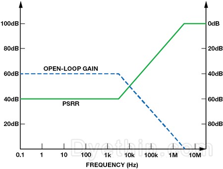
Simplified Plot of LDO Gain vs. PSRR
The picture below shows the three main frequency domains used to characterize the LDO PSRR: the reference voltage PSRR region, the open-loop gain region, and the output capacitance region. The reference voltage PSRR region depends on the PSRR of the reference amplifier and the open-loop gain of the LDO. Ideally, the reference amplifier needs to be completely isolated from power supply disturbances, but in practice, the reference amplifier only needs to reject power supply noise up to tens of Hz because the error amplifier feedback circuit ensures high PSRR at low frequencies.
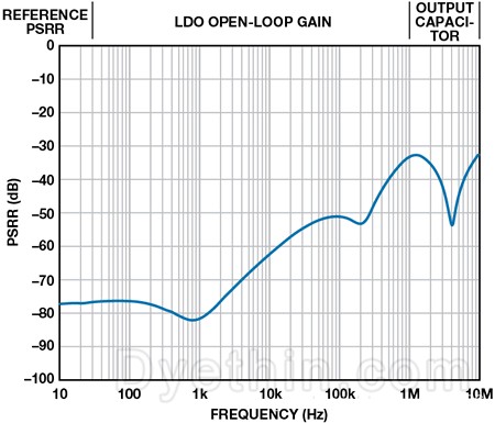
Typical LDO PSRR vs. Frequency
In the second region above about 10 Hz, the PSRR is dominated by the LDO's open-loop gain. The PSRR in this region depends on the error amplifier's gain bandwidth (up to unity gain frequency). At low frequencies, the AC gain of the error amplifier is equal to the DC gain. The gain remains constant until the 3 dB cutoff frequency is reached. Above the 3 dB cutoff frequency, the error amplifier's ac gain decreases with increasing frequency, typically at a rate of 20 dB/decade.
Above the error amplifier's unity gain frequency, feedback from the control loop has no effect on PSRR, which is determined by the output capacitance and any parasitics between the input and output voltages. At these frequencies, PSRR is mainly affected by the ESR and ESL of the output capacitor and the board layout. To reduce the effects of any high-frequency resonance, special attention must be paid to layout.
PSRR vs. Load Current
Load current affects the gain bandwidth of the error amplifier feedback loop and therefore PSRR. At low load currents (typically less than 50 mA), the output impedance of the pass element is high. Due to the negative feedback of the control loop, the output of the LDO is a nearly ideal current source. The pole formed by the output capacitor and pass element occurs at relatively low frequencies, so PSRR tends to increase at low frequencies. High DC gain of the output stage at low currents also tends to increase the PSRR of the error amplifier at frequencies below the unity gain point.
At high load currents, the LDO output cannot approximate an ideal current source. The output impedance of the pass element will drop, causing the gain of the output stage to decrease and the PSRR from DC to the unity gain frequency of the feedback loop to decrease. When the load current increases, PSRR decreases sharply, as shown in Figure 12. When the load current increases from 400 mA to 800 mA, the PSRR of the ADM7150 decreases by 20 dB at 1 kHz.
The output stage bandwidth increases with the output pole frequency. At high frequencies, PSSR should improve as bandwidth increases, but in practice, high-frequency PSRR may not improve because the overall loop gain decreases. Generally speaking, the PSRR at light load is better than that at heavy load.
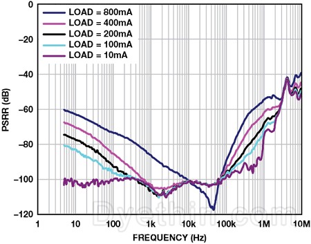
ADM7150 Power Supply Rejection vs. Frequency (VOUT = 5 V, VIN = 6.2 V)
The relationship between PSRR and LDO margin
PSRR is also related to the input-to-output voltage difference (i.e., headroom). For a fixed headroom voltage, PSRR decreases as load current increases; this is especially noticeable at high load currents and small headroom voltages. The image below shows the difference in PSRR versus headroom voltage for a 5 V ADM7172 at a 2 A load.
As the load current increases, the pass element (the PMOSFET of the ADM7172) comes out of saturation and enters the linear operating region, with a corresponding decrease in gain. This causes the overall loop gain of the LDO to decrease and therefore the PSRR to decrease. The smaller the headroom voltage, the greater the gain reduction. At certain small headroom voltages, the control loop has no gain at all and PSRR drops almost to 0.
Another factor that contributes to reduced loop gain is the non-zero resistance RDSON of the pass element. Any voltage drop across RDSON caused by the load current will reduce the effective margin of the pass element. For example, if the pass element is a 1 Ω device, the headroom will be reduced by 200 mV when the load current is 200 mA. When the LDO operates with a headroom voltage of 1 V or less, this voltage drop must be considered when estimating PSRR.
In dropout mode, PSRR is determined by the pole formed by RDSON and the output capacitor. At very high frequencies, PSRR is limited by the ratio of the output capacitor ESR to RDSON.
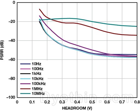
ADM7172 Power Supply Rejection vs. Headroom (VOUT = 5 V, 2 A Load Current)
Compare LDO PSRR specifications
When comparing the PSRR specifications of LDOs, make sure that the measurements are made under the same test conditions. Many older LDOs only specify PSRR at 120 Hz or 1 kHz, with no mention of headroom voltage or load current. At a minimum, the PSRR in the electrical specification sheet should be listed for different frequencies. For a meaningful comparison, it is best to use the typical operating performance curves of PSRR at different loads and headroom voltages.
The output capacitance also affects the LDO PSRR at high frequencies. For example, a 1 μF capacitor has 10 times the impedance of a 10 μF capacitor. At frequencies above the error amplifier's unity-gain crossover frequency, the attenuation of power-supply noise is related to the output capacitance, and the capacitance value is particularly important at this time. When comparing PSRR data, the output capacitors must be of the same type and value, otherwise the comparison will be invalid.
Output noise voltage
Output noise voltage is the RMS output noise voltage over a given frequency range (typically 10 Hz or 100 Hz to 100 kHz) at constant output current and ripple-free input voltage. The primary sources of output noise for LDOs are the internal reference and error amplifier. Modern LDOs operate with internal bias currents in the tens of nA to achieve quiescent currents of 15μA or less. These low bias currents require the use of bias resistors up to the GΩ level. Output noise typically ranges from 5 μV r ms to 100 μV rms. Figure 14 shows the relationship between ADM7172 output noise and load current.
Some LDOs, such as the ADM7172, can use an external resistor divider to set the output voltage above the initial set point, allowing a device initially set to 1.2 V to provide a 3.6 V output voltage. For such applications, a noise reduction network can be added to the voltage divider to restore the output noise to a level close to the original fixed voltage.

ADM7172 Output Noise vs. Load Current
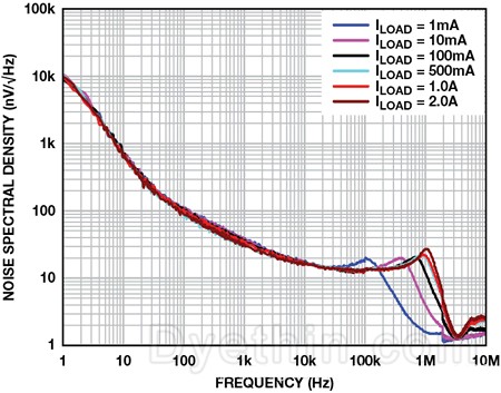
Another representation of LDO output noise is the noise spectral density. Plot the rms noise over a 1 Hz bandwidth at a given frequency over a wide frequency range and then use this information to calculate the rms noise at the given frequency bandwidth. Figure 15 shows the noise spectral density of the ADM7172 from 1 Hz to 10 MHz.
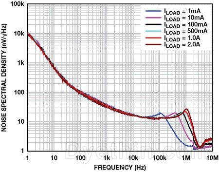
ADM7172 Noise Spectral Density vs. Load Current
Summary
Advantages of LDO include:
(1) Simple structure, few peripheral components, and easy to use.
(2) There is no switching noise and can be used in analog circuits that require high precision and low noise.
But the shortcomings are also obvious:
(1) It can only lower the voltage, not increase it.
(2) Low efficiency, especially when the input voltage is high, and generally used when the load current is less than 1A.
Articles you may also like
Working principle of field Mosfet transistor triode
Basic knowledge and working principle of AC to DC converter
A Method for Optimizing the Gate Drive of SiC MOSFETs
Brief Analysis of Capacitance in AC Circuit