













- Strona główna
- Blogs
- Power management
- A Method for Optimizing the Gate Drive of SiC MOSFETs
A Method for Optimizing the Gate Drive of SiC MOSFETs
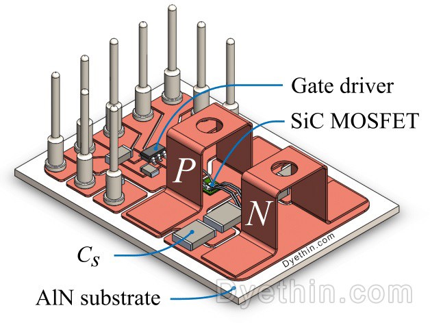
In comparison to conventional silicon MOSFETs and IGBTs, silicon carbide (hence referred to as "SiC") MOSFETs have clear advantages in high-voltage switching power supply applications. Silicon MOSFETs can be utilized for very high voltages (>1000 V). However, they cannot be used for high-frequency (hundreds of kHz) switching. IGBTs are capable of operating at high voltages, but their delayed turn-off and "tail current" restrict their employment to low-frequency switching applications. The best of all worlds is provided by SiC MOSFETs, which allow high-frequency switching at high voltages. However, SiC MOSFETs have particular needs for the gate drive circuit because of their distinctive device properties. With this knowledge, the designer can choose a gate driver that enhances switching performance and device dependability. The properties of SiC MOSFET devices and their gate drive circuit requirements are covered in this article, after which we propose an IC solution that takes these and other system-level factors into account.
SiC MOSFET properties
In comparison to silicon devices, SiC MOSFETs have higher internal gate resistance and lower transconductance (gain), and their gate turn-on thresholds can be lower than 2 V. As a result, the SiC MOSFET needs to have a negative gate-source voltage (usually -5 V) given to it in the off state. SiC devices typically need a gate-source voltage of 18 V to 20 V to lower the on-state resistance (RDS) in the on-state. Low VGS SiC MOSFET operation may result in thermal stress or high RDS failure. Other low gain effects have a direct impact on a number of crucial dynamic switching characteristics, such as on-resistance, gate charge (Miller plateau), and overcurrent (DESAT) Protect, which must be taken into account when building a suitable gate drive circuit.
ON resistance
Due to a confluence of internal device features, the on-resistance vs. junction temperature characteristics of some SiC devices appear to be parabolic* at low VGS. (*This is relevant to M1 and M2 SiC MOSFETs from ON Semiconductor.) When VGS = 14 V, RDS seems to exhibit a negative temperature coefficient (NTC) characteristic, meaning that the resistance drops as the temperature rises. Because of this special property of SiC MOSFETs, which is directly related to their low gain, catastrophic damage may occur if two or more SiC MOSFETs are operated in parallel at low VGS (negative temperature coefficient). SiC MOSFETs should only be operated in parallel when VGS is high enough to guarantee consistent positive temperature coefficient operation or when VGS is more than 18 V.
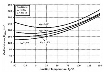
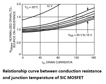
At all VGS and temperature ranges, next-generation M3 SiC has a positive temperature coefficient.
The Gate Charge
The charge is delivered to the SiC MOSFET to accelerate the rise of the gate-source voltage (VGS) from VGS (MIN) (VEE) and VGS (MAX) (VDD). The VGS vs. gate charge (QG) curve can be used to calculate the amount of charge that has to be transmitted for a particular VGS because the device's internal capacitance is not linear. SiC MOSFETs have a "Miller plateau" that is not as flat as silicon MOSFETs and occurs at greater VGS. Due to the device's low gain and the uneven Miller plateau, VGS is not constant in the relevant charge range. It's also important to note that QG = 0 nC, the charge needed to totally discharge the gate of a SiC MOSFET, does not occur at VGS = 0 V. Rather, VGS must be negative (-5 V in this example).
Our curves only show the increase in Qg (also known as the accumulation of Qg or the change in Qg) since we are interested in measuring the amount of charge needed to switch the SiC MOSFET on or off. Another name for this value is Qg. This might be perplexing. This graph must be interpreted in terms of the energy needed, not just the energy contained in the gate-source capacitor.
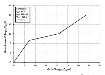
To minimize leakage current in the off state, a negative gate drive blocking voltage is typically used. The low transconductance gain is partially to blame for this. Switching losses, particularly during turn-off, are decreased by using a negative blocking voltage. As a result, it is advised to utilize a minimum VGS of -5 V VGS (MIN) -2 V in the off state for practically all SiC MOSFETs, while some manufacturers specify values as low as -10 V.
Undervoltage defense
Overcurrent detection for DESAT protection comes from the IGBT drive circuit. Upon turning on, the collector-emitter voltage increases, and the whole collector current flows if the IGBT is unable to maintain saturation (referred to as "desaturation"). This obviously has a negative impact on efficiency and, in the worst scenario, may result in the IGBT failing completely. The so-called "DESAT" function keeps track of the IGBT's collector-emitter voltage and alerts the user when a potentially harmful condition arises. SiC MOSFETs have a somewhat different failure mechanism, but a similar circumstance will exist where VDS may increase as the maximum ID flows. The maximum VGS during turn-on may be too low, the gate drive turn-on edge may be too slow, a short circuit may exist, or an overload condition may exist, all of which can result in this undesired state. When the ID load is full, RDS will rise and abruptly drive up VDS. VDS responds swiftly to a SiC MOSFET undersaturation event while the maximum drain current passes through the rising on-resistance. The safeguard may be turned on when VDS hits a specific threshold. Sensing VDS should be done with extra caution to prevent delays, which can hide this occurrence. DESAT is a crucial auxiliary protection for the gate drive circuit as a result.
Automatic switch
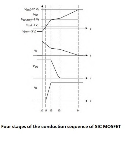
In both the on and off stages of SiC MOSFETs, there are 4 distinct phases. Ideal operating conditions are illustrated by the dynamic switching waveforms. In reality, however, the actual waveform can be significantly impacted by package parasitics, including lead and bond wire inductance, parasitic capacitance, and PCB layout. The performance of SiC MOSFETs used in switching power supply applications must be optimized by careful device selection, ideal PCB layout, and consideration of well-designed gate drive circuits.
Gate Drive Circuit Design Requirements
The SiC gate drive circuit must meet the following crucial criteria in order to effectively make up for the device's low gain and achieve fast switching.
● The majority of SiC MOSFETs perform at their peak when the driving voltage is between -5V > VGS > 20V. For the greatest variety of devices, the gate drive circuit should be able to endure VDD = 25 V and VEE = -10 V.
● VGS needs to have rising and falling edges that happen quickly (within a few ns).
● The ability to deliver high peak gate sink and source currents (a few A) throughout the whole Miller plateau region.
● For high sink current capability, a very low impedance hold or "clamp" must be given when VGS falls below the Miller plateau. The sink current rating must be greater than the amount of current needed to completely discharge the SiC MOSFET's input capacity. High-performance half-bridge power supply topologies should be compatible with a peak sink current minimum rating of about 10 A.
● VDD at the UVLO level, which satisfies the prerequisite of VGS > 16 V before switching starts.
● The monitoring feature of the VEE UVLO guarantees that the negative voltage rails are within allowable bounds.
● The long-term, reliable functioning of SiC MOSFETs is made possible by a desaturation function that is capable of fault detection, reporting, and protection.
● Low parasitic inductance that enables high-speed switching.
● Small size driver package, SiC MOSFET arrangement is as close as possible.
Gate Drivers' Plan
The NCP51705 from On Semiconductor is a SIC gate driver IC with high design flexibility and integration that is compatible with almost anything. The following general-purpose gate driver ICS shares features with CP51705:
● Positive supply voltage for the VDD up to 28 V;
● High peak output current with a source and sink of 6 A and 10 A;
● An integrated 5 V reference for biasing low power loads (such as digital isolators, optocouplers, microcontrollers, etc.) that draw less than 5 V and 20 mA;
● Separate connections for the power and signal grounds;
● Separate output pins for the source and sink;
● Thermal shutdown prevention built-in;
● Distinguishing non-inverting and inverting TTL inputs from PWM inputs.

However, the IC incorporates a number of distinctive properties that make it possible to create dependable SiC MOSFET gate drive circuits with the least amount of external parts. These activities include of:
● Protection from Undervoltage (DESAT);
● Charge pumps (used to set the negative voltage rail);
● UVLO, or programmable Undervoltage lockout.
● Synchronization and problem reporting in digital form;
● 24-pin, 4mm by 4mm, thermally improved MLP package that is simple to integrate at the board level.
Summarize
SiC MOSFETs' low gain makes it difficult for designers to choose the right gate driver IC. SiC MOSFETs can't be driven effectively and consistently by generic low-side gate drivers. The NCP51705 blends a number of features to offer designers a straightforward, high-performance, high-speed solution for safely and effectively driving SiC MOSFETs.
Articles you may also like
Principles and applications of LDO
Working principle of field Mosfet transistor triode
Basic knowledge and working principle of AC to DC converter
Brief Analysis of Capacitance in AC Circuit