


- 홈
- Blogs
- Internet of Things
- RS485 chip selection and instructionsRS485 chip selection and instructions
RS485 chip selection and instructionsRS485 chip selection and instructions
The American Electronics Industries Association (EIA) ratified the RS-485 balanced gearbox standard in 1983. EIA originally prefixed the standard with RS (Recommended Standard), but later modified RS to EIA/TIA to make it easier to identify the standard's source. Although engineers and application guides continue to refer to the standard as RS-485, the official name of the specification is now TIA-485.
As protocol, time, serial or parallel data, and links are all determined by the designer or a higher layer protocol, RS-485 is just an electrical standard that describes the physical layer of the interface. Using balanced (also known as differential) multipoint gearbox lines, RS-485 specifies the electrical properties of drivers and receivers.
Crucial elements
● Noise immunity is raised and noise radiation is decreased through differential transmission.
● Long-distance connections up to 4000 feet (1219 metres), around
● Up to 10Mbps data rate (within 40 inches, or 12.2 metres)
● On the same bus, various drivers and receivers may connect.
● With a wide common-mode range, driver and receiver can have different ground potentials, providing a maximum common-mode voltage of -7 to 12 volts.
Signal Level
The use of differential signals for transmission is primarily responsible for the long-distance transmission capabilities of RS-485. The difference between the two on the line can still be used for judgement when there is noise interference, preventing noise from interfering with the transmitted data.

The next 2 signals are included in the RS-485 differential line:
● A: Non-inverting signal, in A.
● B: Signal inversion
Additionally, a third signal might exist, and for the balanced line to function normally, all balanced lines must have a common reference point known as SC or G. The transceiver will utilise this signal as a benchmark for determining the voltage on the AB line because it has the potential to limit the common mode signal received by the receiving end. According to the RS-485 standard,
● If MARK (logic 1), line B's signal voltage is greater than line A's.
● If SPACE (logic 0), line A's signal voltage is greater than line B's.
Although different ICs employ various signal labelling techniques, the EIA standard only uses the names of signals A and B. Signals B and A will be stronger when the data is 1. Signal B, however, is a "inverted signal" because the standard also states that signal A is a "non-inverted signal." Consequently, signal A and B definitions are more ambiguous. The naming principle of A/B is improperly used by many component manufacturers, therefore the precise definition must actually refer to the chip handbook of the design manufacturer.
One style of naming that is frequently used to avoid conflict is:
● Instead of B (signal 1 is high), use TX+/RX+ or D+.
● Instead of using A (signal 0 is low), use TX-/RX- or D-.
The voltage variations on the U+ terminal and U terminal when RS-485 sends a character using the "asynchronous start-stop" approach (0xD3, the lowest bit is sent first), are shown in the figure below.

Threshold voltage
Line A voltage is higher than line B voltage (VOA>VOB) if the transmitter input receives a logic high level (DI=1); line A voltage is higher than line B voltage (VOB>VOA) if the transmitter input receives a logic low level (DI=0). The receiver outputs a logic high level (RO=1) if the voltage on line A of the receiver is greater than the voltage on line B (VIA-VIB>200mV), and a logic low level (RO=0) if the voltage on line A of the receiver is higher than the voltage on line B.

A driver that complies with the RS-485 standard can emit a differential signal that is no less than 1.5 volts (under a 54 ohm load), and a receiver that complies with the standard can detect input differential signals as low as 200 millivolts. Even with severely damaged cables and connectors, these two values offer enough headroom for highly dependable data transfers.

(UL) Unit load
Depending on their load characteristics, the maximum number of drivers and receivers on the RS-485 bus may vary. In relation to the unit load, driver and receiver loads are measured. A gearbox bus may only have 32 unit loads linked to it, according to the 485 standard.
The unit load is specified as either a steady-state load of 0.8mA current in a -7V common-mode voltage environment or a load of 1mA current in a 12V common-mode voltage environment. When the transceiver is supplied with 1mA and the receiver's input impedance is 12 k, this can be regarded as a unit load. Some RS-485 receivers are rated for 1/4 or 1/8UL, allowing for the mounting of more connections. The following graph illustrates the relationship between receiver input impedance and UL:
| Unit load | Nodes | Minimum receiver input impedance |
| 1 | 32 | 12KΩ |
| 1/2 | 64 | 24KΩ |
| 1/4 | 128 | 48KΩ |
| 1/8 | 256 | 96KΩ |
Working style
There are two possible designs for the bus interface:
● RS-485 Half-duplex (Half-Duplex)
● RS-485 Full-duplex (Full-Duplex)
Data can only be transferred in one direction at a time in numerous half-duplex bus topologies, as indicated in the image below.

The graphic below depicts the full-duplex bus configuration, which enables two-way simultaneous communication between master and slave nodes.

Branch length and bus termination
The data transmission line must have an end point when the cable length is very long in order to prevent signal reflection, and the branch length should be as minimal as possible. The terminating resistor RT, whose value is the characteristic impedance Z0 of the transmission line, must be matched for proper termination. According to the RS-485 standard, the cable's Z0 should be 120. At each end of the cable, the cable trunks are typically terminated with 120 resistors. See the illustration below:

Less than one-tenth of the driver's rising edge time should be the electrical length of the branch (wire distance between the transceiver and the cable trunk):
LStub ≤ tr * v * c/10
Maximum branch length (in feet) is LStub.
driver (10/90) tr rising edge time in nanoseconds
v is the ratio of the speed of light to the pace at which a signal moves along a wire (9.8 * 108 ft/s).
The impedance will be affected by signal transmission reflection if the branch length is too long. The waveforms of long branch length and short branch length are compared in the following figure:

Cable Length and Data Rate
The only cables that can be utilised at high data rates are shorter ones. Low data rates allow the use of longer cables. The DC resistance of the cable limits the cable length for low-speed applications by increasing the voltage drop across the cable and reducing the noise margin. The AC effect of the cable limits the signal quality and cable length when using high-speed applications. A conservative curve for the variation in cable length and data rate is shown in the image below.

Fail-Safe
The receiver outputs are in an indeterminate state while the bus is idle and no device is driving it. Random data is then transmitted across the UART as a result of this, which can result in erroneous start bits or framing issues. Pull-up and pull-down resistors can be installed on the bus for biassing in order to address this issue. For information on the precise size of the pull-up and pull-down resistors, as illustrated in the following picture, please refer to the RS-485 bias pull-up and pull-down resistor values:

Following are the calculations for R1 and R2 (assuming RT=120):
R1=R2=R
VIA-VIB ≥ 200mV
VIA-VIB = RT*VCC / (2R+RT) = 200mV
if VCC = 5V,then R = 1440Ω
if VCC = 3V,then R = 960Ω
The system has a higher noise margin if the R value is lower (VIA-VIB>200mV). The pull-up and pull-down resistors will inevitably result in DC current bias, a higher Tx load, and fewer nodes. The graph below displays the bus state and differential input voltage:

Receivers that truly fail-safe
Pull-up and pull-down resistors are no longer required because a new generation of RS-485 receivers has been modified to allow the differential input threshold voltage to be changed from 200 mV to -200 mV and -30 mV. When the bus is not in use, the receiver output is high (RO=1) and in an asserted condition when VIA-VIB=0 (higher than -30mV).


Isolation
Since RS-485 typically employs a lengthy link, the nodes on the bus will have slightly varied ground levels. Common mode interference will be overlaid on the transmission line when there is a significant ground potential difference. It is extremely risky to rely on the local ground as a current loop if the superimposed interfering signal exceeds the common mode range of the receiver input. To accomplish reliable long-distance transmission, it is best to use signal and power isolation. The isolated RS -485 chip wiring diagram for the ADI ADM2485 is shown in the illustration below:

ESD defence
Large transient voltages can be produced in industrial settings by lightning strikes, power fluctuations, and electrostatic discharges, which can harm RS-485 transceivers. For RS-485 applications, the following ESD protection, EFT protection, and surge protection requirements are applicable:
IEC 61000-4-2 ESD protection
IEC 61000-4-4 EFT protection
IEC 61000-4-5 surge protection
A TVS diode or other external clamping device can be used to further increase the level of protection. In RS-485 applications, TVS clamps the bus voltage to the RS-485 transceiver's common-mode voltage range (-7 to 12 volts). RS-485Y applications are the exclusive focus of some TVS devices. A resistor RS (10-20) can be placed between the protected device and the input pin for further protection against larger power supply transients.


Articles you may also like
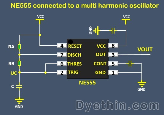
NE555 datasheet and Pinout, NE555 circuits generates square waves

RS485 chip selection and instructions

Hall Effect Sensors & Switches
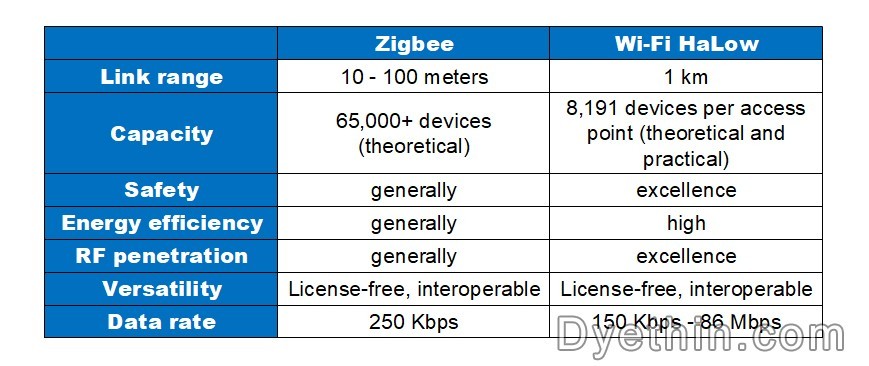
IoT Connectivity - Wi-Fi HaLow Vs Zigbee


