














- Home
- Blogs
- Internet of Things
- NE555 datasheet and Pinout, NE555 circuits generates square waves
NE555 datasheet and Pinout, NE555 circuits generates square waves

1. What is NE555 timer?
The NE555 timer IC is a highly stable integrated circuit belonging to the 555 series of timing ICs, commonly used in timers, pulse generators, and oscillation circuits. This IC was released by Signals Corporation around 1971 and was the only very fast and commercialized Timer IC at that time. Due to its ease of use, low cost, and good reliability, it is still widely used in the design of electronic circuits to this day.
The NE555 timer mainly consists of a comparator, SR latch, R-S trigger, digital to analog converter, and other parts. Due to its excellent performance, it is widely used in various timing control circuits, such as stable oscillators, monostable triggers, PWM generators, slope integral A/D conversion, etc.
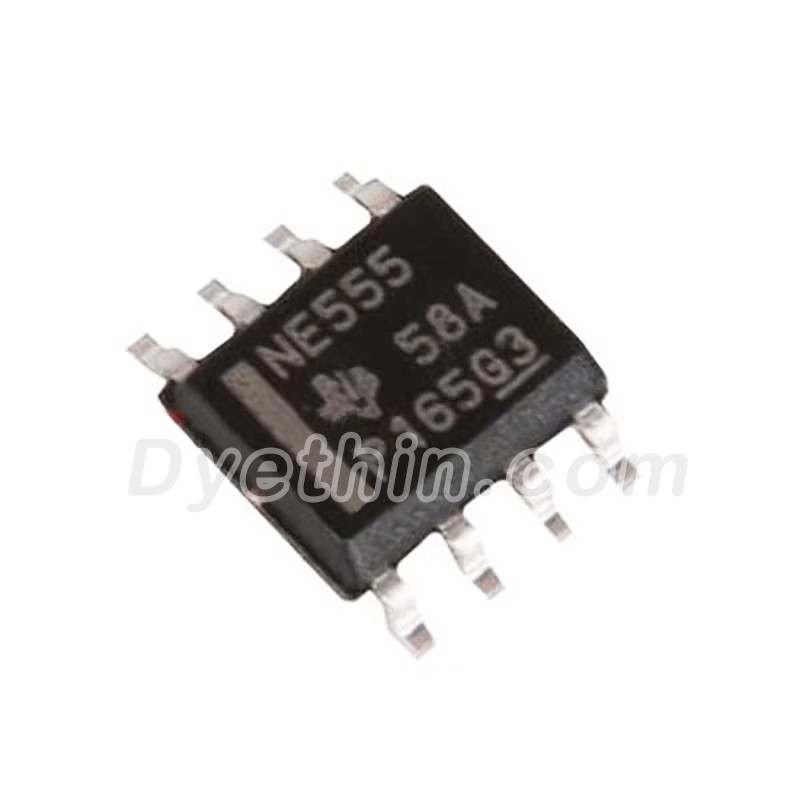
2. NE555 Features
From the data table of NE555, we can know that IC 555 has the following characteristics
● Timing From Microseconds to Hours
● Astable or Monostable Operation
● Adjustable Duty Cycle
● TTL-Compatible Output Can Sink or Source
● Up to 200 mA
● On Products Compliant to MIL-PRF-38535,All Parameters Are Tested Unless Otherwise Noted. On All Other Products, Production Processing Does Not Necessarily IncludeTesting of All Parameters.
3.Applications
● Fingerprint Biometrics
● lris Biometrics
● RFID Reader
Data from NE555 spec sheet
4. NE555 Pinout
We can obtain its pinout information from the NE555 spec sheet
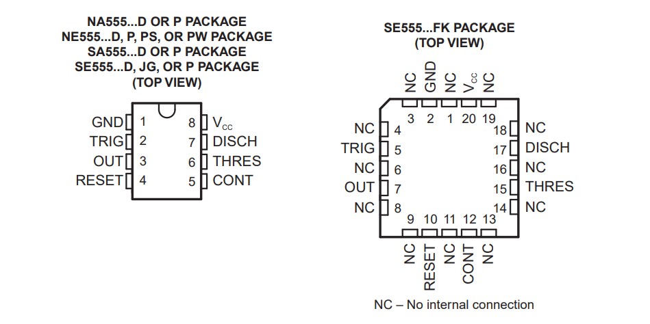
NE555 Pinout
NE555 Pin Functions
| PIN FK NO. | DESCRIPTION | |||
| CONT | 5 | 12 | 1/O | Controls comparator thresholds,Outputs 2/3 VCC,allows bypass capacitor connection |
| DISCH | 7 | 17 | Open collector output to discharge timing capacitor | |
| GND | 1 | 2 | - | Ground |
| NC | 1, 3,4,6,8,9,11,13,14,16,18, 19 | - | No internal connection | |
| OUT | 3 | 7 | High current timer output signal | |
| RESET | 4 | 10 | Active low reset input forces output and discharge low. | |
| THRES | 6 | 15 | End of timing input.THRES>CONT sets output low and discharge low | |
| TRIG | 2 | 5 | Start of timing input.TRIG<½CONT sets output high and discharge open | |
| Vcc | 8 | 20 | - | Input supply voltage, 4.5 V to 16 V.(SE555 maximum is 18 V) |
5. Usage of NE555 IC
Power connection: The NE555 IC can operate at a power supply voltage of 4.5V to 18V. VCC is connected to the positive pole, and GND is connected to the negative pole.
Timing function: By connecting resistors and capacitors to the corresponding pins, the NE555 IC can be configured to be used as a timer.
Trigger and reset: The NE555 IC can be placed in the trigger or reset state through external circuits to achieve different functions.
Output: The NE555 IC has an open drain output that can drive LEDs, relays, or other loads.
6. NE555 circuits usage tips
Stability: To ensure the stability of the circuit, it is recommended to use resistors and capacitors with a precision of 1%.
Power decoupling: Add a 0.1 between VCC and GND μ The ceramic capacitor of F can improve the stability of the circuit.
Protect output: To protect the output of the NE555 circuits from damage, an appropriate current limiting resistor can be added.
Extended functionality: Through innovative design of external circuits, more complex functions can be achieved, such as adjustable duty cycle and frequency.
7. Advantages and disadvantages of NE555
Advantages:
Multifunctionality: The NE555 can be configured to achieve various functions, such as timers, pulse generators, and oscillators.
Wide power supply voltage range: can operate at a power supply voltage of 4.5V to 18V.
Affordable price: As NE555 has been produced for decades, its price is relatively low.
Easy to use: The required functions can be achieved through simple external component connections.
Disadvantages:
Limited speed: Compared to modern microcontrollers, the NE555 has limited speed.
Temperature stability: Its performance may be affected by temperature.
Single function limitation: Although its functionality can be extended through external circuits, its single function capability may be limited compared to dedicated ICs.
8. NE555 alternatives and selection suggestions
Alternative: Modern microcontrollers or other specialized ICs can be considered as substitutes for NE555 to achieve more complex and high-speed functions.
Selection suggestion: When selecting an alternative model, factors such as required functionality, speed, power supply voltage range, size, and cost need to be considered. Ensure that the selected model meets practical application requirements and provides better performance and stability. For example, if complex functions or high-speed applications need to be implemented, modern microcontrollers can be chosen; If only simple timing or pulse functions are needed, and cost is a factor to consider, then NE555 is still a good choice.
9. Generating square waves using NE555 circuits
Firstly, let's take a look at the internal structure of the NE555 circuits:
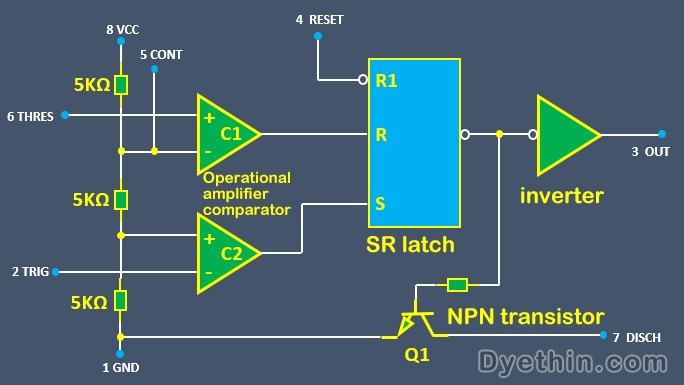
C1 and C2 are two operational amplifier comparators, and the internal resistance values of these three resistors are the same, all 5K ohms. The one behind is an SR latch, the one behind is an inverter, and there is also an NPN transistor inside.
Let's take a look at the basic parameters. From the resistance voltage divider, we can know that the voltage VI1 at the same phase end of comparator C1 is 2/3VCC, and the voltage VI2 at the opposite phase end of C2 is 1/3VCC. Everyone should know that the output of an operational amplifier comparator is VCC when the voltage at the same phase end is greater than the voltage at the opposite phase end, and 0 when the voltage at the same phase end is less than the voltage at the opposite phase end.
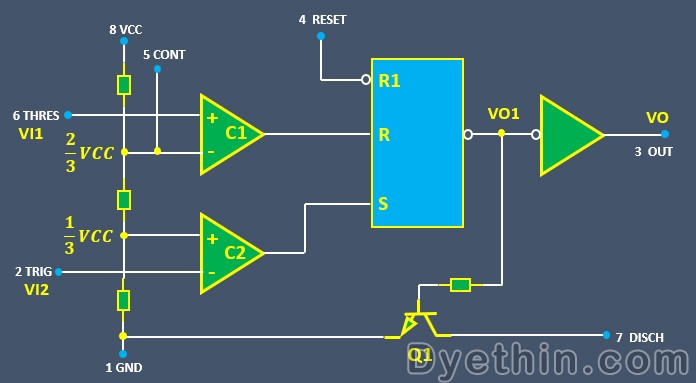
For this SR latch
| SR Latch Input Output Relationship Table | |||||
| RESET | S | R | VO1 | VO | Q1 |
| 0 | / | / | 1 | 0 | ON |
| 1 | 1 | 0 | 0 | 1 | OFF |
| 1 | 1 | 1 | 0 | 1 | OFF |
| 1 | 0 | 0 | Maintain the previous state | Maintain the previous state | Maintain the previous state |
| 1 | 0 | 1 | 1 | 0 | ON |
| NE555 Input Output Relationship Table | |||||
| RESET | VI2 | VI1 | VO1 | VO | Q1 |
| 0 | / | / | 1 | 0 | ON |
| 1 | <1/3VCC | <2/3VCC | 0 | 1 | OFF |
| 1 | <1/3VCC | >2/3VCC | 0 | 1 | OFF |
| 1 | >1/3VCC | <2/3VCC | Maintain the previous state | Maintain the previous state | Maintain the previous state |
| 1 | >1/3VCC | >2/3VCC | 1 | 0 | ON |
NE555 circuits can be used to connect Schmitt triggers, monostable triggers, and multi harmonic oscillators.
To generate square waves, NE555 circuits needs to be connected to a multi harmonic oscillator. Let's take a look at the circuit diagram, everyone

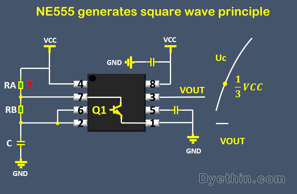
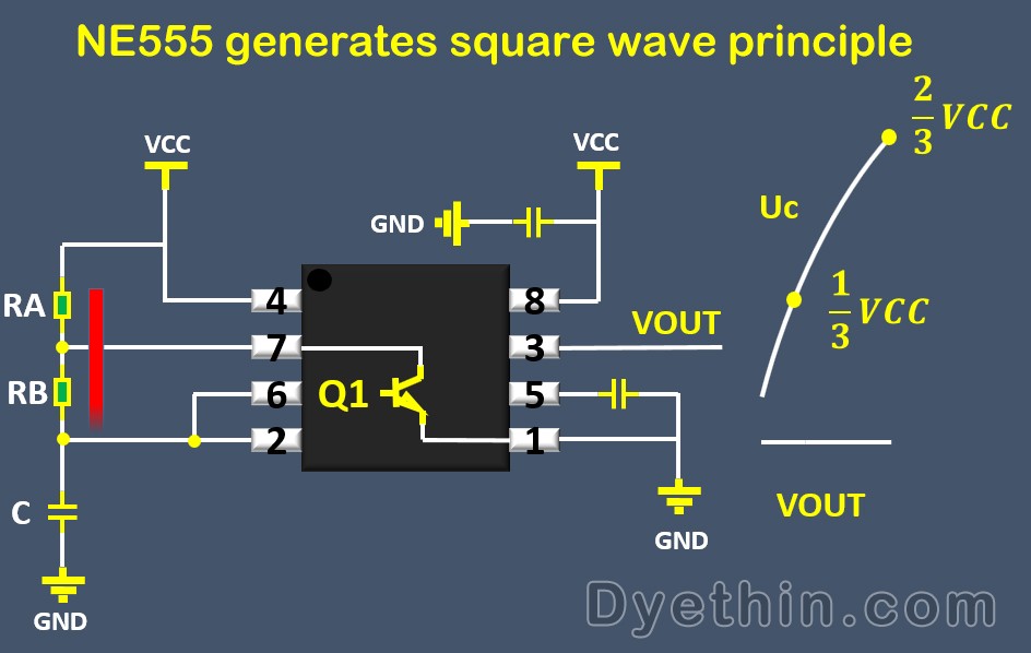
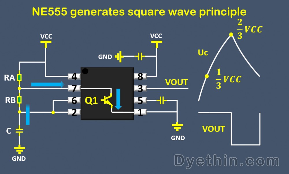
This circuit mainly needs to understand the charging and discharging circuit diameter of the capacitor. When charging a capacitor, it is charged through R1 and R2. When discharging, when Q1 conducts, the capacitor is discharged through R2.
When charging capacitors, when VI1=VI2<1/3VCC, VO=1, Q1 is turned off,
When 1/3VCC< VI1=VI2<2/3VCCtime, VO=1,
When VI1=VI2>2/3VCC, VO=0, Q1 conducts, and the capacitor discharges. When 1/3VCC<VI1=VI2<2/3VCC, VO=0,
When the discharge is placed at VI1=VI2<1/3VCC, VO=1, Q1 is turned off, and the capacitor is charged,
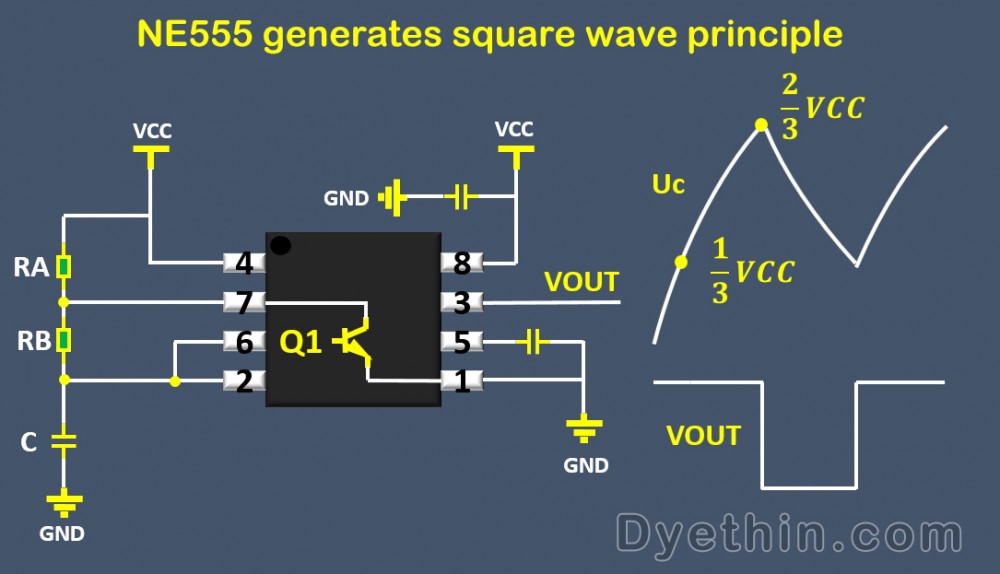
By repeatedly charging and discharging in this way, the output VO will output a square wave.
Let's take a look at parameter calculations.
Calculation formula for capacitor charging from V1 to V2
The time t for the capacitor to charge from V1 to V2 is RC * l n ((VCC-V1)/(VCC-V2))
The time it takes for the capacitor to discharge from V1 to V2
T=RC * ln (V1V2)
Charging time/square wave high-level time
T1=(RA+RB) * C * ln2
Discharge time/square wave low-level time
T2=RB * C * ln2
cycle
T=(RA+2RB) C * ln2
Duty cycle
Q=(RA+RB)/(RA+2RB)
Everyone can see from the formula of this duty cycle that the duty cycle of this square wave is fixed and not adjustable. In order to obtain an adjustable duty cycle, we need to separate the charging and discharging paths of the capacitor. The following circuit is obtained.
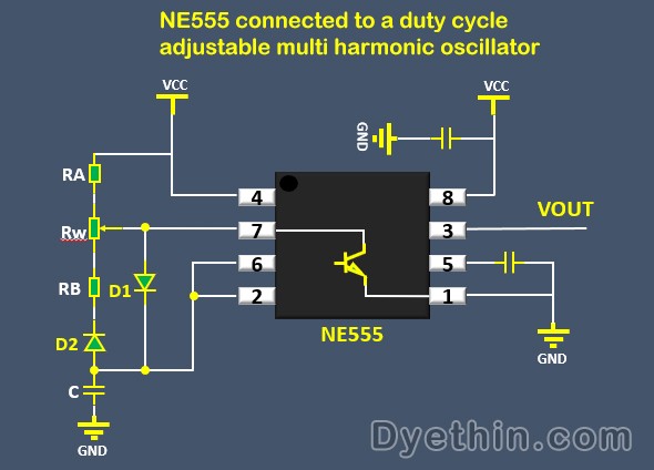
The charging path is this,
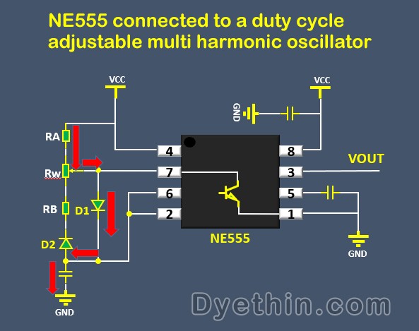
The discharge path is this,
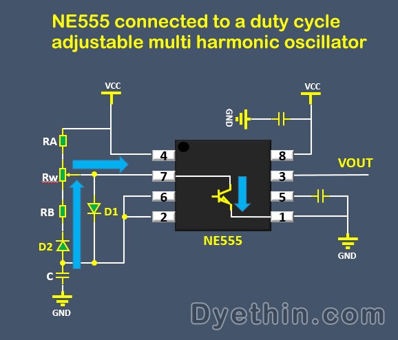
We can change the duty cycle of the output square wave by adjusting the position of the center tap of the potentiometer. The parameters of this circuit are as follows:
Charging time/square wave high-level time T1=(RA+Rw1) * C * ln2
Discharge time/square wave low-level time T2=(RB+Rw2) * C * ln2
Cycle T=(RA+RB+Rw) C * ln2
Duty cycle q=(RA+Rw1)/(RA+RB+Rw)

Articles you may also like

Hall Effect Sensors & Switches
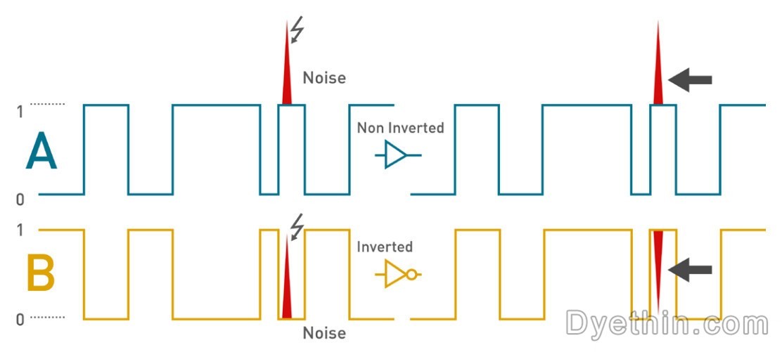
RS485 chip selection and instructions
RS485 chip selection and instructionsRS485 chip selection and instructions
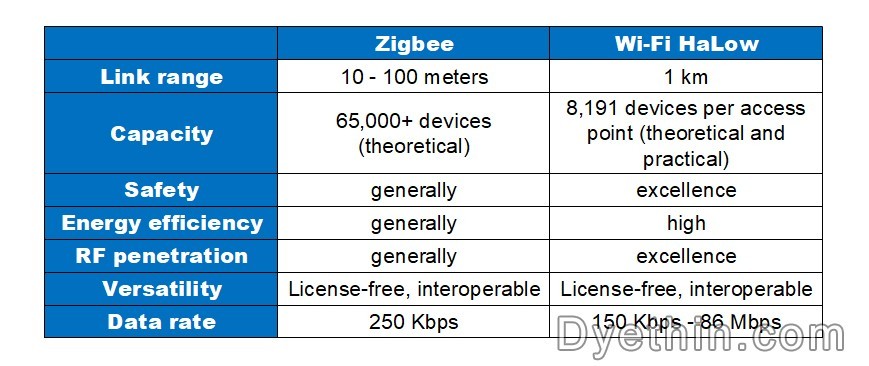
IoT Connectivity - Wi-Fi HaLow Vs Zigbee

-
-
-
-
-
-
-
-
-
stmicroelectronics
ARM® Cortex®-M4 STM32G4 Microcontroller IC 32-Bit Single-Core 170MHz 128KB (128K x 8) FLASH 100-LQFP (14x14)