













- Home
- Blogs
- Semiconductor
- What Is a Transistor? How It Works & Common Uses
What Is a Transistor? How It Works & Common Uses
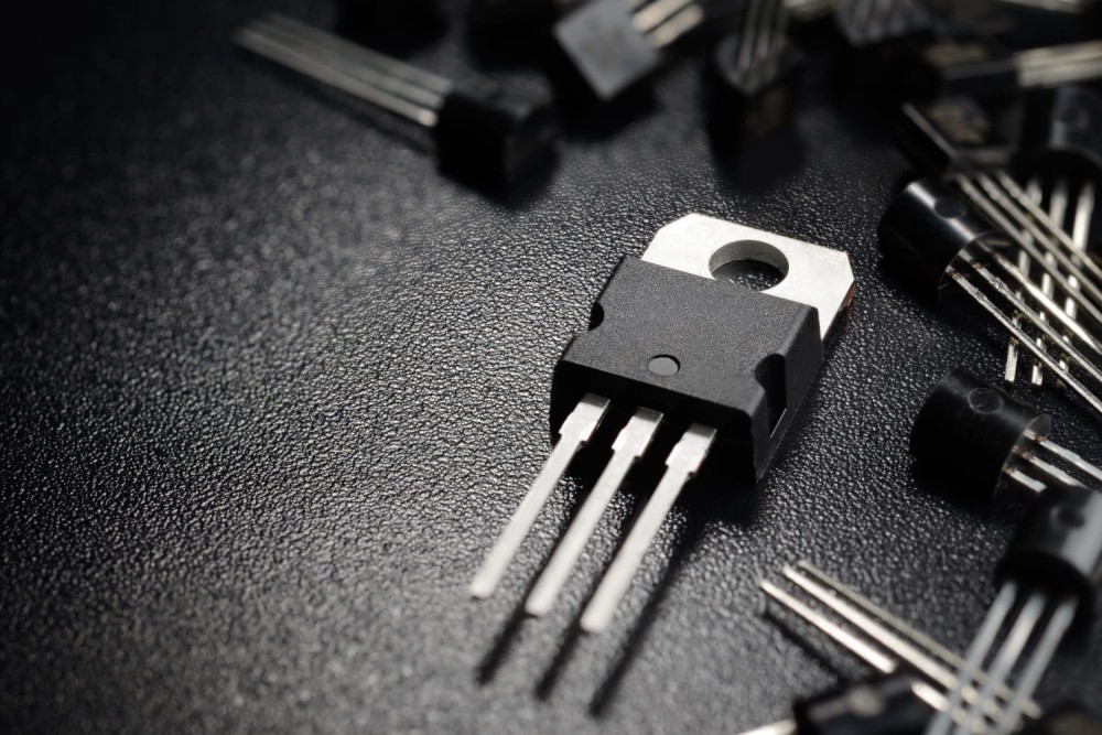
Your smartphone contains somewhere north of 15 billion transistors. Not components in total, transistors specifically. That makes the transistor the single most manufactured object in human history, produced at a rate that makes every other manufactured good look trivial.
So what is a transistor, exactly, and why does it matter which one you choose for your circuit?
This article works through the definition, the symbol, both operating modes, and the four main transistor families, with enough specificity to support real component decisions.
What Is a Transistor Made Of?
A transistor is a semiconductor device that controls the flow of electrical current. It does this in one of two ways: by amplifying a weak signal into a stronger one, or by acting as a switch – toggling between a conducting state and a blocking state.
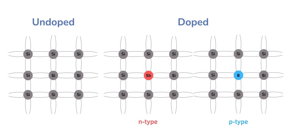
Most transistors are made from silicon, though some use germanium or gallium arsenide. Silicon on its own doesn't conduct electricity well. Doping (the deliberate introduction of impurities into the silicon lattice) gives it either extra electrons (creating an n-type semiconductor) or electron "holes" (creating a p-type semiconductor). Combining these regions in specific arrangements is what makes transistor behavior possible.
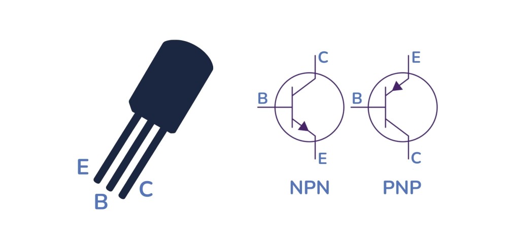
Most discrete transistors used in basic circuit design have three terminals. In a BJT, they're called the Base, Collector , and Emitter . In a FET, they're the Gate, Drain, and Source. The names differ, but the principle is the same: a small signal at one terminal controls a much larger current between the other two . That leverage is what makes transistors so useful, and those three terminals each have a specific visual shorthand on a schematic.
How Do You Read a Transistor Symbol?
Misreading the transistor symbol on a schematic leads directly to ordering the wrong part. The symbol tells you the transistor type, the carrier direction, and the terminal arrangement before you ever open a datasheet.
For BJT transistors , the symbol shows three terminals with a vertical line (the base) and two angled lines (the collector and emitter). The emitter always has an arrow. That arrow is the key: it points away from the base in an NPN transistor, and toward the base in a PNP transistor. The arrow follows conventional current flow.
FET symbols look different. The gate is separated from the semiconductor body by a gap (for MOSFETs) or connected directly (for JFETs), and the terminals are labeled Gate, Drain, and Source. An arrow on the body line indicates channel type – pointing inward for N-channel, outward for P-channel.
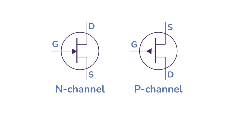
Quick rule: On any BJT symbol, the arrow points in the direction of conventional current flow through the emitter. On FET symbols, the arrow indicates channel polarity.
How Do Transistors Work?
The two operating modes are the right place to start – everything else follows from them. How transistors work depends on which mode the circuit is designed around.
As a Switch
The transistor operates in either cutoff (fully off) or saturation (fully on). A small signal at the control terminal, the base or gate, opens a much larger current path between the other two terminals. Digital circuits rely entirely on this behavior. Every logic gate, memory cell, and processor instruction comes down to transistors switching on and off at extremely high speeds. A modern CPU executes billions of these switching events per second.
As an Amplifier
Here, the transistor stays in its active (linear) region rather than snapping to an extreme. A small variation in the input signal produces a proportionally larger variation at the output. The transistor draws energy from the supply voltage to build up the output, keeping the original waveform shape intact. This is how hearing aids boost faint sounds, how radio receivers pull usable signals from background noise, and how audio amplifiers drive speakers from a line-level signal.
How Current Gets Controlled
In a silicon BJT, the base-emitter junction behaves like a forward-biased diode. Once the base-emitter voltage crosses roughly 0.6–0.7V , carriers begin injecting from the emitter into the thin base region. Most of those carriers sweep through to the collector before recombining. The ratio of collector current to base current is the transistor's current gain (written as hFE or β), and it varies widely by device class: power BJTs can fall as low as 10–15, general-purpose types like the 2N3904 or BC547 land between 100 and 400, and high-gain small-signal transistors can exceed 600. A small base current controls a much larger collector current. That's the physics of control in one sentence.
FETs work differently. The gate draws almost no current. Applying a voltage to the gate creates an electric field that controls how much current flows through the semiconductor channel between drain and source. This voltage-controlled behavior is why FETs dominate power and digital applications where driving efficiency matters.
What Are the Main Types of Transistors?
Choosing the right transistor means matching the device to the demands of the circuit. Types of transistors differ in how they're controlled, how much power they handle, and how fast they switch. Here's how each type compares in practice.
BJT Transistors (Bipolar Junction Transistors)
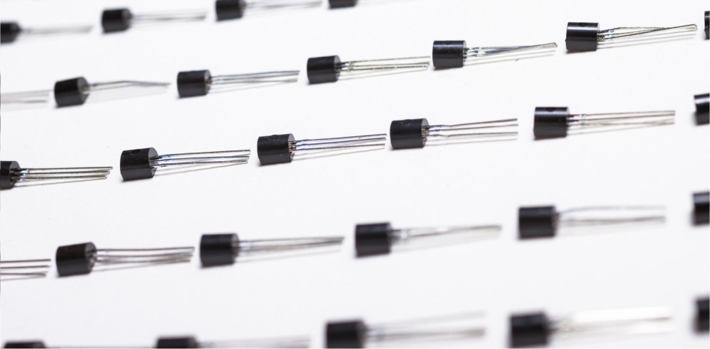
BJTs are current-controlled devices . A current flowing into (or out of) the base drives a larger current between the collector and emitter. They come in two configurations: NPN , where current flows from collector to emitter when the base is driven high, and PNP , where the logic is inverted.
BJTs are well-suited to audio amplification, signal processing, and low-to-medium power switching . They're predictable, widely available, and straightforward to bias. The tradeoff is that the base always draws some current, which adds to drive circuit complexity, and switching speeds are lower than FETs at high frequencies.
Browse BJT transistors at Dyethin for NPN and PNP single devices across a wide range of gain and voltage ratings.
MOSFET and FET Transistors
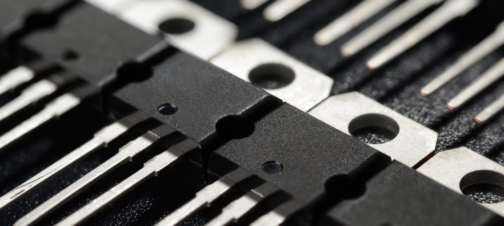
MOSFETs are voltage-controlled devices . The gate is insulated from the semiconductor channel by a thin oxide layer, which means gate current is essentially zero. Applying a voltage above the threshold turns the device on; removing it turns the device off. That insulated gate makes MOSFETs far more efficient to drive than BJTs.
MOSFETs are the dominant choice for high-speed switching, power conversion, motor control, and digital logic . N-channel MOSFETs are more common due to higher electron mobility; they switch faster and have lower on-resistance for the same die size. The gate behaves like a small capacitor , which means high-frequency applications need attention to gate drive design to avoid slow or incomplete switching.
Dyethin stocks MOSFET and FET transistors across a range of voltage ratings and packages, from signal-level devices to high-side power switches.
JFET Transistors (Junction Field-Effect Transistors)
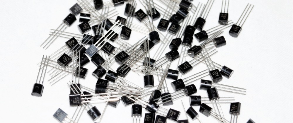
JFETs are voltage-controlled, depletion-mode devices . Unlike MOSFETs, their gate is a reverse-biased PN junction rather than an insulated oxide. They're on by default and pinch off as the gate-source voltage increases in magnitude, the opposite of how enhancement-mode MOSFETs behave.
Where JFETs earn their place is in low-noise analog circuits . They offer extremely high input impedance and some of the lowest noise figures available in a discrete transistor. Precision instrumentation, front-end RF amplifiers, electrometer circuits, and audio preamps where signal integrity is non-negotiable are natural JFET territory. They're less common in power or digital roles, but for precision analog work, nothing else in the discrete transistor world comes close.
Find JFET transistors at Dyethin suited to low-noise analog front-end design.
IGBT Transistors (Insulated Gate Bipolar Transistors)
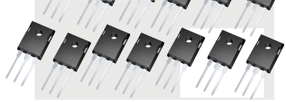
IGBTs are hybrid devices – engineered to combine the best of both major transistor families. The input gate structure is borrowed from the MOSFET (voltage-controlled, low gate drive current), and the output stage behaves like a BJT (capable of sustaining high current at high voltage). The result is a device that handles power levels neither type could manage as well on its own.
IGBTs are the standard choice for high-voltage, high-current applications : electric vehicle inverters, solar and wind power converters, industrial motor drives, UPS systems, and induction heating equipment. Where a standard MOSFET's on-resistance becomes prohibitive at voltages above a few hundred volts, IGBTs maintain efficient operation into the kilovolt range. Switching speed is the limitation – conventional silicon IGBTs in hard-switching power applications rarely exceed 20–30 kHz before switching losses become prohibitive, and modern fast-switching variants extend that range to roughly 40 kHz. MOSFETs can operate orders of magnitude faster at comparable voltage, which is why silicon carbide (SiC) MOSFETs are displacing IGBTs in newer high-frequency power designs.
Dyethin carries IGBT transistors in a range of voltage and current ratings for high-power discrete applications.
Each of these four families has its own subtypes, packaging variants, and specification nuances. For a full side-by-side comparison of ratings, switching behavior, and application fit, see our guide on Types of Transistors .
Where Are Transistors Used in Everyday Devices?
Theory gives you the vocabulary. A look at where each transistor type appears in real products makes the selection logic concrete.
Digital computing depends on CMOS technology, complementary pairs of N-channel and P-channel MOSFETs wired so only one conducts at a time. When the output is stable, neither transistor conducts, and the current draw drops to near zero. Only during the transition from one state to the other does current briefly flow. At a circuit level, this is why a smartphone with billions of transistors can run for hours on a battery that would drain in minutes if those transistors drew continuous current. A modern smartphone processor integrates upward of 19 billion transistors on a die around 60mm2 (roughly half the area of a thumbnail).
Power conversion exposes a tradeoff that doesn't appear in low-power circuits: every switching event (turn-on and turn-off) dissipates energy, and those switching losses multiply with frequency. At 10 kHz, an IGBT's switching losses are manageable; at 50 kHz, they can exceed conduction losses and push junction temperatures beyond safe limits. This is what sets the practical operating frequency for a given device in a real inverter stage, not just the datasheet spec. It also explains the shift toward SiC MOSFETs in next-generation EV drivetrains. SiC switches at higher frequencies with lower switching losses, allowing smaller, lighter magnetic components in the inverter.
Audio amplification in class AB stages pairs two BJTs in a push-pull configuration. One handles the positive half of the waveform, the other the negative half. Where the two handoff introduces crossover distortion if their hFE values are mismatched, which is why matched transistor pairs are specified in quality amplifier designs rather than pulling two parts from a bulk bin. Thermal runaway is a related failure mode specific to BJTs as temperature rises, VBE drops, and collector current increases, generating more heat in a feedback loop. Properly designed bias networks, with a temperature-tracking diode or thermistor, compensate for this, but it is a genuine failure mode absent in MOSFET-based amplifier stages.
RF and wireless circuits are where the noise figure (NF) specification drives transistor selection. NF quantifies how many decibels of noise the transistor adds to the signal it amplifies. Every decibel added at the first amplifier stage (the LNA, or low-noise amplifier) gets carried through and amplified by every subsequent stage in the receive chain, degrading sensitivity across the board. A 1 dB improvement at the input has more impact on receiver performance than a 10 dB improvement later in the chain. This is why transistor selection for the LNA stage receives disproportionate attention in the design of GPS receivers, cellular base stations, and radio telescopes.
Motor control uses MOSFETs or IGBTs in H-bridge configurations, where four transistors switch in diagonal pairs to reverse current direction through the motor winding. The non-obvious constraint here is dead time, which occurs when one diagonal pair turns off, and the opposite pair turns on. Both pairs must be fully off simultaneously for a brief window (typically 100–500 nanoseconds) to prevent a direct short across the supply rails. Too little dead time causes shoot-through current; too much causes torque ripple at low speeds. Gate driver ICs enforce this timing automatically in most production designs, but the dead-time value is a tuned parameter that affects both efficiency and motor smoothness.
Sensor signal conditioning rarely gets the spotlight, yet it's where front-end transistor selection has the most direct impact on measurement accuracy. At microvolt signal levels, two noise specs matter: voltage noise (measured in nV/√Hz) and current noise (measured in pA/√Hz). BJTs have lower voltage noise but higher input current noise. A problem when the source impedance is high, because current noise multiplied by source impedance becomes voltage noise. JFETs have far lower input current noise, making them the better fit for high-impedance sources like piezoelectric sensors, pH electrodes, and photodiodes. A poor transistor choice at this stage introduces noise that no downstream correction can recover.
Which Transistor Type Is Right for Your Next Project?
A transistor is a three-terminal semiconductor device that controls current, but that one-sentence definition covers a lot of ground. The BJT, MOSFET, JFET, and IGBT each approach the control problem differently, and each is optimized for a different set of conditions. What transistors are at a conceptual level is the starting point. Which transistor suits your voltage, current, frequency, and drive circuit requirements is where the actual design work gets done.
Related articles

FAQs
Articles you may also like
Characteristics of CPU, GPU, and FPGA
Silicon controlled rectifier (SCR) and switch control circuit explained
Accurately measure resistor value using ADC
The difference between RAM ROM FLASH

-
-
-
-
-
broadcom-limited
Precision isolation amplifier with 15kV/μs CMTI and ±1% gain accuracy
-
-
-

-