


- Accueil
- Blogs
- Power management
- Explanation of PFC working principle
Explanation of PFC working principle
Overview
After the AC power supply on the input side is full-wave rectified, a large capacitor is typically connected to obtain a relatively flat DC voltage in conventional applications. The rectifier-filter circuit consists of both nonlinear and energy storage components. Consequently, despite the sinusoidal nature of the input AC voltage, the input AC current is severely distorted and appears pulse-like. As depicted below:

A large number of rectifier circuits will produce distorted non-sinusoidal currents at the grid end, resulting in severe consequences. Harmonic currents have a very negative impact on the grid, and the power factor at the input end of the apparatus will be drastically diminished. Similarly, for AC-DC applications, the DC output terminal typically requires a stable DC bus voltage, which must be even be adjustable.
Therefore, the application of PFC serves three principal purposes:
A) Improve harmonics of input current
B) Improve input PF value
C) Stable output voltage
Fundamental analysis
This section uses the widely applicable CCM Boost PFC to illustrate the fundamental working principle of the power factor correction circuit (PFC). The diagram in Figure 1 depicts the primary power circuit of a Boost active power factor corrector. The primary circuit includes a single-phase bridge rectifier and a Boost converter (inductor LPFC, switching tube Qp, diode D, and bus capacitor Cbus). The phase-alternating rectifier (rectifier bridge) converts the input alternating positive and negative alternating current into steamed bread waveform direct current (without negative value), and the post-stage BOOST circuit converts the steamed bread waveform DC voltage into a pulsating amount controlled by a particular duty cycle. Small and stable bus DC voltage while ensuring that the inductor current on the input side presents a sinusoidal current consistent with the waveform envelope of the input voltage.

Enhanced topology analysis
The core of the PFC circuit consists of a BOOST circuit, as shown in Figure 1. Before investigating the PFC topology and control, it is necessary to analyze the
BOOST circuit's operating principle and control logic.
When the DC converter circuit is operating in BOOST mode, the output voltage V is greater than the input voltage Vg, as depicted in Figure 2 below. Vg represents the input DC power supply voltage, L represents the Boost inductor, Q represents the BOOST switch tube, which is activated with a specific duty cycle d, D represents the freewheeling diode, C represents the output filter capacitor, R represents the load resistance, and V represents the output voltage.

When the switch is switched on and off, the BOOST circuit operates in different modes, and the current and voltage waveforms of each key node are distinct due to the different working states. Consequently, the working state procedure of the Boost circuit can be separated into two types based on the working state of the MOS in the BOOST circuit.
1) Working status 1
The equivalent circuit of the MOS transistor Q when it is activated is depicted in Figure 3 below. Both extremities of the inductor L through Q are directly loaded with the input DC voltage Vg. The inductor voltage is equal to the input voltage Vg, and the inductor current increases linearly. The current course is depicted in the diagram. Figure 2.6 depicts the driving waveform and the inductor current waveform. Due to the conduction of Q, the MOS tube clamps the anode of diode D to ground, diode D is reversely turned off, and capacitor C continues to power the output load R.

In functioning state 1, the input power supply serves as the inductor's energy storage. At this juncture, the inductor current and input voltage Vg satisfy:

2) Working status 2
The freewheeling diode D is activated when the MOS transistor Q is turned off because the inductor current cannot be forced to commutate in the preceding stage. If the conduction tube voltage drop of the freewheeling diode D is disregarded, the voltage at both ends of the inductor L is, where the voltage is greater than that, and the inductor current decreases linearly. The direction of the current is depicted in Figure 2.5, along with the driving waveform and the inductor current waveform.

In the second state of operation, the inductor discharges energy while the input power supply Vg compensates for the energy lost by the output capacitor in the previous stage. At this juncture, the input voltage, output voltage, and inductor current satisfy the following conditions:

Figure depicts the BOOST circuit switch tube drive and inductor current:

In a switching cycle, if the on-time for Q is ton, the off-time is toff, the switching cycle time of PWM is TPWM, and the duty cycle is defined as D, then:

In one switching cycle, per the inductance energy balance theorem:

Then, when operating in BOOST mode, the relationship between input voltage, output voltage, and duty cycle can be calculated:

BOOST circuit double closed-loop control
Typically, the output constant voltage closed-loop control of BOOST utilizes the control structure depicted in Figure 6: voltage outer loop and current interior loop. The voltage outer loop is a slow loop, whereas the current inner loop is a rapid loop, and their control bandwidths differ by an order of magnitude.
After the output voltage V has been converted, it is sent along with the reference voltage (target voltage) Vref to the voltage loop calculation. When the output voltage is detected to be less than Vref, the output of the voltage loop increases after the calculation of the voltage outer loop; conversely, when the output voltage is detected to be greater than Vref, the output of the voltage loop decreases after the calculation of the voltage outer loop.
Current inner loop receives the output of the voltage outer loop and the inductor current conversion. The overall control logic is as described below. When the output voltage is detected to be less than Vref, the output of the voltage loop increases after the calculation of the voltage outer loop, resulting in an increase in the reference current Iref. During the calculation of the current inner loop, the output control amount of the current loop and the duty cycle increase, thereby increasing the inductor current and the output voltage; however, when the output voltage is detected to be greater than Vref, the output of the voltage loop decreases. In other words, the reference current decreases. After the calculation of the current inner loop, the output control amount and duty cycle of the current loop diminish, causing the inductor current and output voltage to decrease.

Principles of PFC operation and control logic
Conventional PFC control consists of two closed-loop control methods, namely output voltage loop and current loop. The function of the voltage loop is to ensure the stability of the DC bus voltage on the output side, while the function of the current loop is to ensure the sinusoidal envelope of the input inductor current. As depicted in Figure 8, the simplified PFC operating principle is a line.

PFC operates as follows: the output voltage Vbus is compared with the reference voltage Vref, and the output value Vr of the voltage loop is calculated; this value is then multiplied by the Boost input voltage Vdc to produce the current reference value iref in the form of a steamed bun wave. The reference current iref is compared to the switching current is, and the switching tube's duty cycle signal d is obtained after passing through the current loop. The switching tube is controlled after the driving circuit so that the waveform of the input current (i.e., the inductor current iL) is identical to that after rectification. Essentially, the waveform of the voltage waveform Vdc is identical.
The above control strategy demonstrates that when the output voltage is less than the reference voltage Vref, the voltage loop output Vr rises, that is, the reference current value iref rises after passing through the multiplier, and the duty cycle of the switch tube rises under the influence of the current loop, causing the output voltage to increase adjust.
The figure below depicts the waveforms of the input voltage Vdc, the inductor current iL corrected by Vi, and the input current ii. The input current is modulated by the PWM frequency, transforming the original pulse-shaped waveform into a waveform that closely resembles sinusoidal (including high-frequency ripple). In the circuit depicted in the figure, when the switch tube is turned on, io = 0 and iL = is; when the switch tube is turned off, is = 0 and iL = io, and the current through the switch tube is is. Waveform, input current with high-frequency ripple, can be approximated as a uniform sine wave by taking the average value of each switching cycle.

Articles you may also like

Principles and applications of LDO
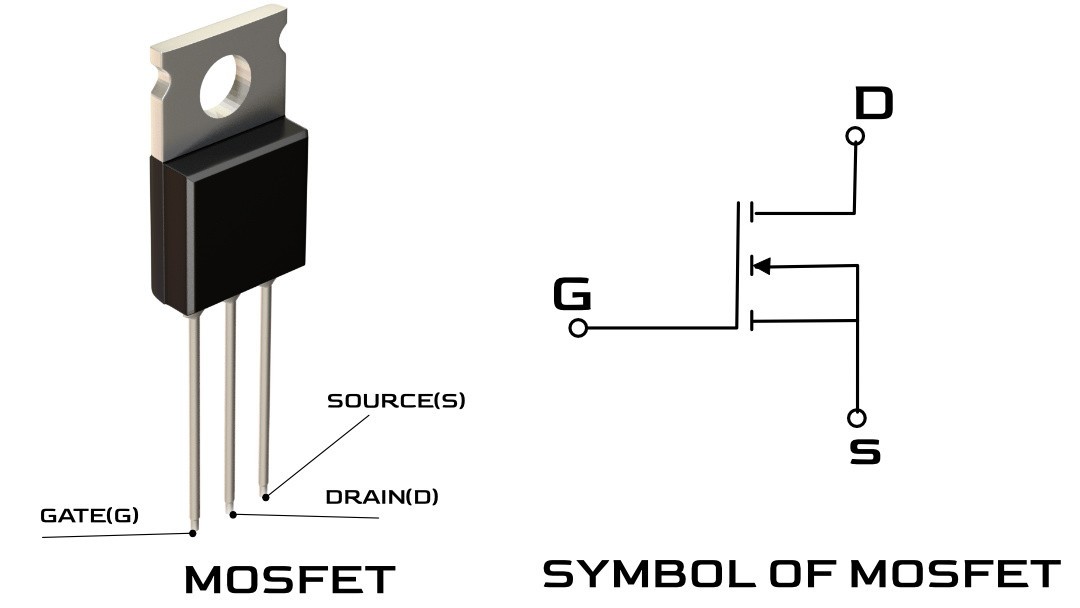
Working principle of field Mosfet transistor triode
Basic knowledge and working principle of AC to DC converter
A Method for Optimizing the Gate Drive of SiC MOSFETs


