


- Home
- Blogs
- Power management
- DC-DC elements of layout (1)
DC-DC elements of layout (1)
PCB layout design is as essential to the design of switching power supplies as circuit design. A reasonable layout can prevent numerous power supply circuit-related issues. The superposition of output and switching signals may result from an unreasonable layout, resulting in increased noise, poor regulation performance, poor stability, etc. With appropriate design, these issues can be avoided.
1. DC-DC circulation

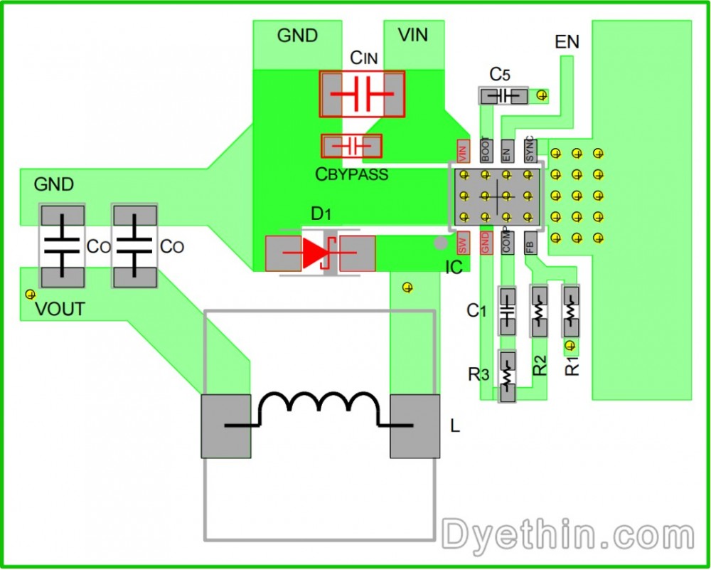
Figure 24-1 illustrates the current path when switching element Q1 is activated.
The red line in Figure 24-1 represents the primary current, its path, and its flow direction when the toggling element Q1 is activated. Cbypass is a high-frequency decoupling capacitor, whereas CIN is a capacitance of considerable size. When the switching element Q1 is activated, a sharp current flows, the majority of which is supplied by Cbypass, followed by CIN, and the steadily varying current is supplied by the input power source.

Figure 24-2 depicts the current path when toggling element Q1 is deactivated.
Figure 24-2's red line illustrates the current path when the toggling element Q1 is disabled. The freewheeling diode D1 is activated, releasing the energy stored in the inductor L to the output side. Due to the inductor's series relationship with the output topology of the buck converter, the output capacitor's current fluctuates but is relatively steady.

Important paths in terms of current differential, layout, as shown in Figure 24-3
Figure 24-3's crimson line represents the difference between Figures 24-1 and 24-2. When the switching element Q1 transitions from off to on and on to off, the red line's current will fluctuate significantly. Due to the rapid nature of this transition, a waveform with more higher harmonics will be produced. This differential system is a crucial aspect of PCB layout that requires the utmost care.
2. PCB layout key elements
The primary aspects of PCB layout are as follows:
Place the input capacitor, freewheeling diode, and IC chip on the same side of the PCB and as close as feasible to the IC chip.
Consider adding a heat dissipation via array in order to enhance heat dissipation conditions.
The inductance can reduce the switching node's radiated noise, which is only second in importance to the input capacitor. It must be located close to the integrated circuit, and the copper foil area of the inductance wiring should not be excessively enormous.
The output capacitor should be placed as near to the inductor as possible.
The construction of the feedback path should be kept away from noise-generating components such as inductors and freewheeling diodes.
3. Configuration of the input capacitor
First place the input capacitor and the freewheeling diode when designing a circuit layout. When designing a power supply with a low output current (Iout1A), the required input capacitance is typically modest, and a ceramic capacitor can sometimes serve as both CIN and Cbypass. This is because the frequency characteristics of a ceramic capacitor improve with decreasing capacitance value. Please validate the frequency characteristics of the actual product prior to use, as the frequency characteristics of various ceramic capacitors vary.

Frequency characteristics of ceramic capacitors, as shown in Figure 24-4
CIN: 1µF 50V X5R 10µF 50V X5R
CBY: 0.1µF 50V X7R 0.47µF 50V X7R
As depicted in Figure 24-4, when a large-capacity capacitor is used as CIN, its frequency characteristics are typically subpar; therefore, it is typically necessary to configure a high-frequency decoupling capacitor Cbypass with excellent frequency characteristics in parallel with CIN. Surface-mounted multilayer ceramic capacitors (MLCC) with a capacitance between 0.1F and 0.47F are typically utilized for Cbypass.

Figure 24-5 depicts the optimal input capacitor layout.
Due to the influence of wiring parasitic inductance, voltage noise/ringing will be produced if Cbypass, IC VIN pin, and GND pin are separated by a great distance; therefore, it is advisable to reduce the distance between them. Even if Cbypass is located closest to the IC in a buck converter application, there are hundreds of megahertz of high frequencies on the ground of CIN. It is recommended, therefore, that the grounding of CIN and the grounding of the output capacitor Cout be separated by 1 to 2 cm.

When CBYPASS is placed nearest to the same side as the IC, as depicted in Figure 24-6.
If the CIN is situated at a distance of 2cm, there will not be too many issues.

Ripple voltage can be increased by placing CIN on the rear of the IC, as shown in Figure 24-7.

Suboptimal Input Capacitor Layout Increases Noise Due to Vias and Inductance, as Depicted in Figure 24-8.
4. Configuration of the freewheeling diode
Diode D1 should be positioned on the same layer as the IC and in close proximity to the IC terminals. Figure 24-9 depicts the optimal configuration of Cbypass, CIN, and D1 diode. If the distance between the IC pin and the diode is too great, the output will be contaminated with noise pulses caused by the parasitic inductance of the wiring. Using the shortest and widest wiring feasible, the freewheeling diode should be connected directly to the switch pin and the GND pin of the integrated circuit. If vias are used to connect to the bottom layer, the glitch noise will increase due to the parasitic inductance of the vias; therefore, vias must not be used in the wiring of the freewheeling diode.

Figure 24-9: Optimal Freewheeling Diode Configuration
Figure 24-10 demonstrates additional preposterous layouts. The distance between the freewheeling diode and the switch pin and GND pin of the integrated circuit is great, which will increase the parasitic inductance of the wiring and cause larger noise surges. Occasionally, an RC snubber circuit may be added as a last-ditch effort to reduce the malfunction noise resulting from poor layout.
Non-ideal Freewheeling Diode Layout, Figure 24-10
The snubber circuit depicted in Figure 24-11 must be positioned near to the IC's switch pin and GND pin. Due to the parasitic inductance of the wiring, the capacitor cannot absorb glitch noise even when located at both ends of the diode (Figure 24-12).

Figure 24-11 depicts the optimal snubber circuit layout.

Figure 24-12 depicts a suboptimal Snubber circuit configuration.
Thermal Pad 5.
Even though the copper foil of the PCB is helpful for heat dissipation, the area-equivalent heat dissipation effect cannot be attained beyond a certain area because the thickness is insufficient. The use of the substrate to dissipate heat is realized through the substrate's plate, and the use of heat dissipation vias can effectively transmit heat to the opposite side of the substrate, thereby reducing thermal resistance by a significant amount.
For the package in which the heat dissipation pad is exposed at the bottom of the chip, the pad is at ground potential, and laying a wide copper foil trace will not increase electromagnetic interference. To enhance the thermal conductivity of the heat dissipation vias, it is recommended to use an array of small-diameter through-holes with an inner diameter of approximately 0.3 mm that can be electroplated. It is simple for tin to crawl during the reflow soldering process if the hole diameter is excessively large. It is recommended that the spacing of the heat dissipation vias be approximately 1.2mm and that they be positioned directly under the package's heat dissipation pad. If the area directly under the heat dissipation pad is insufficient for heat dissipation, you can also position heat dissipation vias as near as possible to the integrated circuit.
)
Articles you may also like
Principles and applications of LDO
Working principle of field Mosfet transistor triode
Basic knowledge and working principle of AC to DC converter
A Method for Optimizing the Gate Drive of SiC MOSFETs

-

panasonic-electronic-components
63V 47μF SMD aluminum capacitor, 125°C, low ESR, AEC-Q200 qualified
-

-

-

-

-

-

-

-

nexperia-usa-inc
Voltage Level Translator Bidirectional 1 Circuit 2 Channel 100Mbps 8-VSSOP