


How to design PCB heat dissipation holes?
When designing a PCB, there are many situations where we need to dissipate heat for certain components such as linear regulators. In most cases, these designs are general-purpose through-hole assemblies because the heat sink can effectively dissipate heat within the aluminum area and keep the device in cooler ambient conditions. But if we talk about any SMD device, heatsink is not available and most of the time. We must use copper pouring techniques to create adequate heat sinks on the copper layer.
1. What are PCB heat dissipation holes?
The heat dissipation hole is a method of dissipating heat by using a channel (via hole) that penetrates the PCB board to conduct heat to the back. It is arranged directly under the heating element or as close as possible to the heating element.
Heat dissipation holes are a method of using PCB boards to improve the heat dissipation effect of surface mount components. Structurally, through holes are designed on the PCB board.
If it is a single-layer double-sided PCB board, the copper foil on the surface and back of the PCB board is connected to increase the area and volume for heat dissipation, that is, to reduce the thermal resistance.
If it is a multi-layer PCB board, you can connect the surfaces between the layers or limit the partially connected layers, etc. The purpose is the same.

2. How to design PCB heat dissipation holes?
The placement and size of PCB thermal vias vary widely, depending on the type of component, different rules and expertise.

But one main rule is to use heat vents as close to the heat source as possible directly under the heating element. Then in cases where the heat source is not ideal, thermal vias can also be placed on the periphery of the component regardless of component pad placement. In this case, too, the rule remains the same, which is to place the cooling holes as close to the periphery of the group as possible.
To effectively use the heat dissipation holes, it is very important to arrange the heat dissipation holes close to the heating element, such as directly under the component. As shown in the figure below, it can be seen that it is a good method to use the heat balance effect to connect locations with large temperature differences.

PCB thermal via placement example
Example: Thermal via configuration The following is an example of the thermal via layout and size for the HTSOP-J8 package with exposed rear heat sink.
3. How big are PCB heat dissipation holes?
In order to improve the thermal conductivity of the heat dissipation holes, it is recommended to use small-diameter through holes with an inner diameter of about 0.3mm that can be filled by electroplating. It should be noted that if the hole diameter is too large, solder creepage may occur during the reflow soldering process.
The spacing of the heat dissipation holes is about 1.2mm, and they are arranged directly under the heat sink on the back of the package. If just under the heat sink on the back is not enough to dissipate heat, you can also configure heat dissipation holes around the IC. The key point of configuration in this case is to configure it as close as possible to the IC.

Heat dissipation hole size
4. Thermal conductivity of different materials
Thermal conductivity is a key factor in determining how much heat a material can absorb. The following table provides an idea of the thermal conductivity of different materials. With the help of this table, you can have a certain reference
See table below:

Therefore, from the table above, it can be seen that aluminum has worse thermal conductivity than copper. However, because aluminum radiators have a larger area, they produce a more effective cooling effect on heated equipment. However, as we have seen, if copper is used effectively, it can dissipate more heat than the same area of aluminum.
Effective thermal via placement is when vias are used appropriately in an IC or heating element pad using conduction as a heat transfer method where heat is distributed between multiple layers of copper and then through free air, heat dissipation begins using convection method is transmitted through the air. It is recommended that the thermal via inner diameter needs to be smaller, e.g. approximately 0.35 mm. If the hole diameter is larger, incorrect soldering problems with soldering may occur during the reflow process, so extra care needs to be taken. However, if a larger diameter is required, hot filling may help compensate for this.
5. PCB heat dissipation hole design considerations
During the thermal via design process, there are few things that need to be paid attention to. Here are the following 6 suggestions.
a) The exposed pad is designed to transfer heat directly from the case to the copper area. Solder is not very effective as a heat sink because it is so thin and solder does not conduct electricity well.

Thermal vias on U1 exposed pad
The image above shows the thermal vias on the exposed pad of U1.
b) For exposed pad packages, the greatest heat dissipation occurs through the vias to the bottom layer of the PCB and then dissipates into the air. Therefore, the large area of the bottom layer will also reduce the heat dissipation of the component package.
c) Separate the heated components and use heat dissipation holes to dissipate heat, which helps to evenly distribute heat to other packages.
d) Thermal vias are the only source of heat dissipation on DFN and QFN packages since the top layer copper does not have maximum space due to pin assignments. Therefore, with underlying copper, the only way to increase thermal conductivity is to use thermal vias.
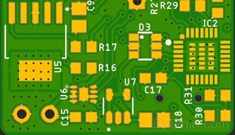
U5 and IC2 use thermal vias. IC2 uses a QFN flat package where thermal vias are only possible as this does not include the larger copper area on the solder layer due to the distribution of the component pads.
e) The effective copper area of the thermal via connection device will be the maximum copper length (independent of the solder layer) that can be directly connected to the component package using thermal vias.
f) The thickness of the copper plane also affects thermal conductivity, 2Oz copper has better heat resistance than 1.0 Oz or 0.5Oz copper.
Here are some suggestions for using heat dissipation holes. I hope it will help engineers who need to consider heat dissipation equipment in their designs.
Articles you may also like
Design of High Current H-Bridge Motor Drive Circuit
The working principle, key parameters, and selection of TVS

Understanding NAND Gate: The Universal Logic Gate in Digital Circuits
Gas Discharge Tube Symbols, Characteristics and Structure


