


- Inicio
- Featured Products
- Texas Instruments
- 74LS161AN Functionality Explained: Funcion, Pinout & Datasheet
74LS161AN Functionality Explained: Funcion, Pinout & Datasheet
74LS161AN is a relatively funcion synchronous 4-bit binary counter IC manufactured by Texas Instruments. The chip belongs to the 74 series of TTL (Transistor-Transistor Logic), which is widely used in digital circuits such as frequency measurements, clock control, timer design and other digital circuits for binary counting, frequency division and other counting-related functions.

74LS161AN Function
Synchronous Binary Counting
Presettable (Preset Counter Initial Value)
Controllable Count Enable Funcion
High-speed operation
The 74LS161AN utilizes TTL logic for high-speed operation capability and stable operation at higher frequencies. Typically, the chip can operate up to 30 MHz.
74LS161AN Main Parameters
Number of bits: 4 bits
Counting order: Upward counting
Operating supply voltage: 4.75V to 5.25V
Minimum/maximum operating temperature: 0°C to +70°C
Output current: High level 8mA, low level -400μA
Package: PDIP-16
Logic family: LS
74LS161AN Pinout Configuration

| Pin No. | Pin Name | Function Description |
| 1 | CLR | Clear input: when the pin is low, all outputs of the counter are reset to zero. |
| 2 | CLK | Clock input, the counter counts when the clock rises. |
| 3 | ENP | The count enable input must be at a high level for the counter to respond to clock pulses. |
| 4 | ENT | Counting enables serial input for cascading multiple counters. |
| 5 | D0 | Pre-set data input bit D0, used to set the initial count value. |
| 6 | D1 | Pre-set data input bit D1. |
| 7 | D2 | Pre-set data input bit D2. |
| 8 | GND | Ground wire. |
| 9 | D3 | Preset data input bit D3. |
| 10 | Q3 | Output bit Q3, high level indicates that the third bit of the binary number is 1. |
| 11 | Q2 | Output bit Q2. |
| 12 | Q1 | Output bit Q1. |
| 13 | Q0 | Output bit Q0. |
| 14 | RC | Carry output, used for cascading counters, indicating that the current count has overflowed. |
| 15 | LD | Preset enables input, and when the pin is low, the counter loads preset data. |
| 16 | VCC | Power input. |
74LS161AN Datasheet
Logic diagram(positive logic)

Reading the 74LS161AN Datasheet is a critical step in gaining an in-depth understanding of the IC's operating principles and electrical characteristics. The Datasheet usually contains the following important information:
Funcion Block Diagram: shows the chip's internal structure and logical relationships.
Electrical Characteristics: A detailed list of the chip's input voltage, output voltage, current consumption and other key parameters.
Timing Diagrams: Timing diagrams show the relationship between the signals of each pin, which helps to understand the behaviour of the chip in different operating modes.
Absolute Maximum Ratings: These values indicate the limits of what the chip can withstand under various conditions; exceeding these values may damage the chip.
74LS161AN Schematic Diagram
The 74LS161AN performs synchronized counting by means of an input clock signal (CLK). Whenever the rising edge of the clock signal arrives, the counter will increment its binary count value if the enable signals (ENP and ENT) are high and the clear signal (CLR) is high. The preset function (LD pin) allows the user to set the output value of the counter to a specific value at any moment, which is useful for applications that require the count to start from a non-zero value.
Function Table

Schematic diagram

Transition diagram

Draw a state transition diagram based on the 161 output changes and synchronized counting conditions.
From the state transition diagram, it can be seen that the circuit has a total of 10 states, and every 10 states run to restore the initial state, so the circuit is a decimal counting circuit.
Multisim simulation results

The simulation result using multisim is shown in Fig.
From the simulation results, it can be found that every ten CLK cycles, the input outputs a low level, which is consistent with the theoretical derivation; the circuit is a decimal addition counter.
74LS161AN Applications
Since the 74LS161AN features synchronized counting, programmable presets, and internal overfeed, it is widely used in a variety of electronic devices and systems, including but not limited to:
- Frequency measurement: By cascading multiple 74LS161AN counters, high-precision frequency measurement circuits can be constructed.
- Clock Control: Used to generate or control clock signals in digital circuit design.
- Timer: Combined with external circuits to realize precise timing function.
- Counter Expansion: The number of bits in the counter can be easily expanded by utilizing its rounding output (RCO) and parallel input function.
Comparison of 74LS161AN Vs 74LS163
Difference: The same 4-bit binary synchronous counter, but different in the clearing method. For example, 74LS163 is synchronous clearing, while 74LS161 is asynchronous clearing.
Common Points: These features include synchronous counting and programmable load control lines.
Precautions for using the 74LS161AN
The following precautions should be taken when using the 74LS161AN in circuit design:
Proper connection of power and ground: Ensure that the VCC and GND pins are properly connected to avoid power supply noise and unstable operation.
Stability of the clock input: The clock signal should remain stable to ensure the accuracy of the counter.
Use of bypass capacitor: Place a bypass capacitor between VCC and GND to minimize the impact of power supply noise on the chip.
Use of Clear Function: Use the CLR pin to clear all counter outputs when the counter is initialized or reset.
Conclusion
As a high-performance four-bit binary synchronous counter chip produced by Texas Instruments, 74LS161AN has a wide range of applications in electronic projects thanks to its synchronous counting, programmable presets and internal overfeed. Through the introduction of this article, I believe the reader has a comprehensive understanding of the 74LS161AN chip's funcion characteristics, pin configuration and application scenarios. In practical applications, it is recommended to combine with Datasheet for detailed design to ensure the stability and reliability of the circuit.
Related articles
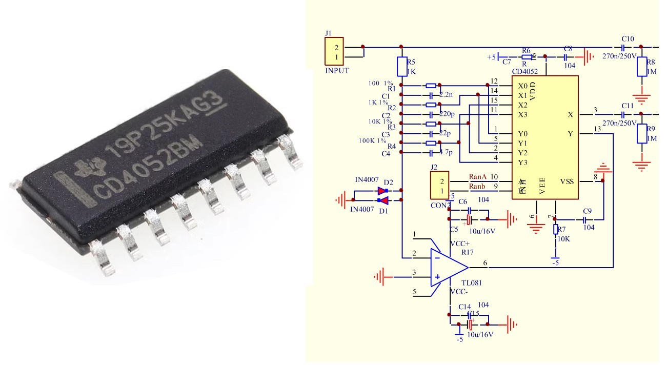
Logic IC CD4052 Comprehensive understanding and usage guide
MAX485 is an RS 485/RS422 transceiver integrated circuit IC produced
P75NF75 Mosfet Datasheet, Pinout, Equivalent, Voltage, Circuit and Uses
LM2596 datasheet, pinout, and Design LM2596 DC DC module
BC547 NPN transistor usage case and explanation of BC547 Datasheet and BC547 pinout
FAQs
Articles you may also like
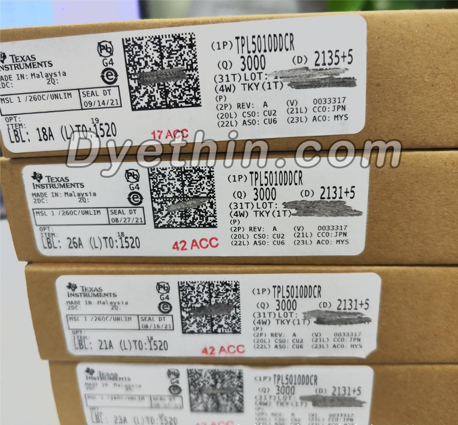
TPL5010 hardware watchdog circuit
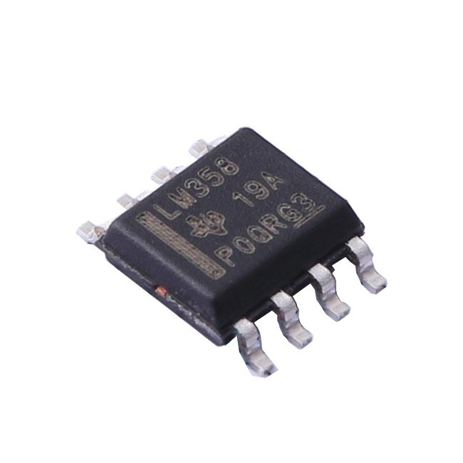
Operational amplifier IC LM358 pinout diagram and functions
Logic IC CD4052 Comprehensive understanding and usage guide
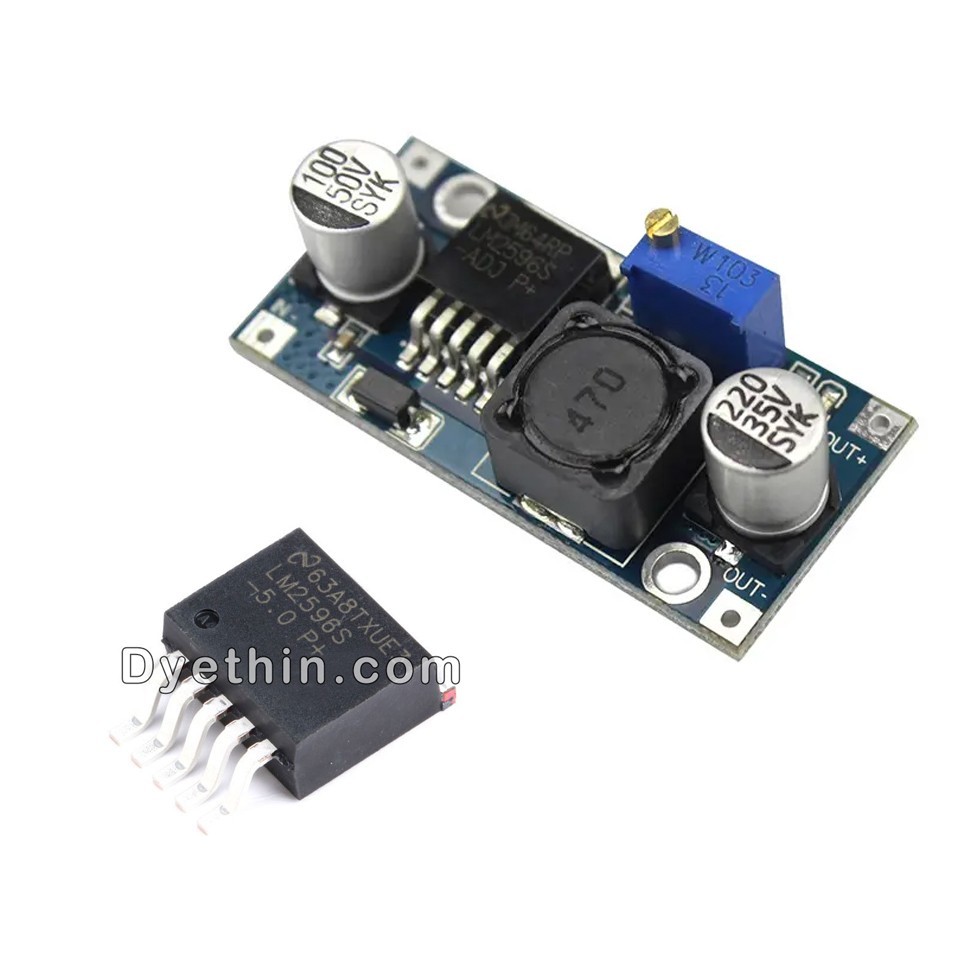
LM2596 datasheet, pinout, and Design LM2596 DC DC module


