













- Startseite
- Blogs
- Basic knowledge
- What is the internal structure of FPGA?
What is the internal structure of FPGA?
FPGA Structure Overview

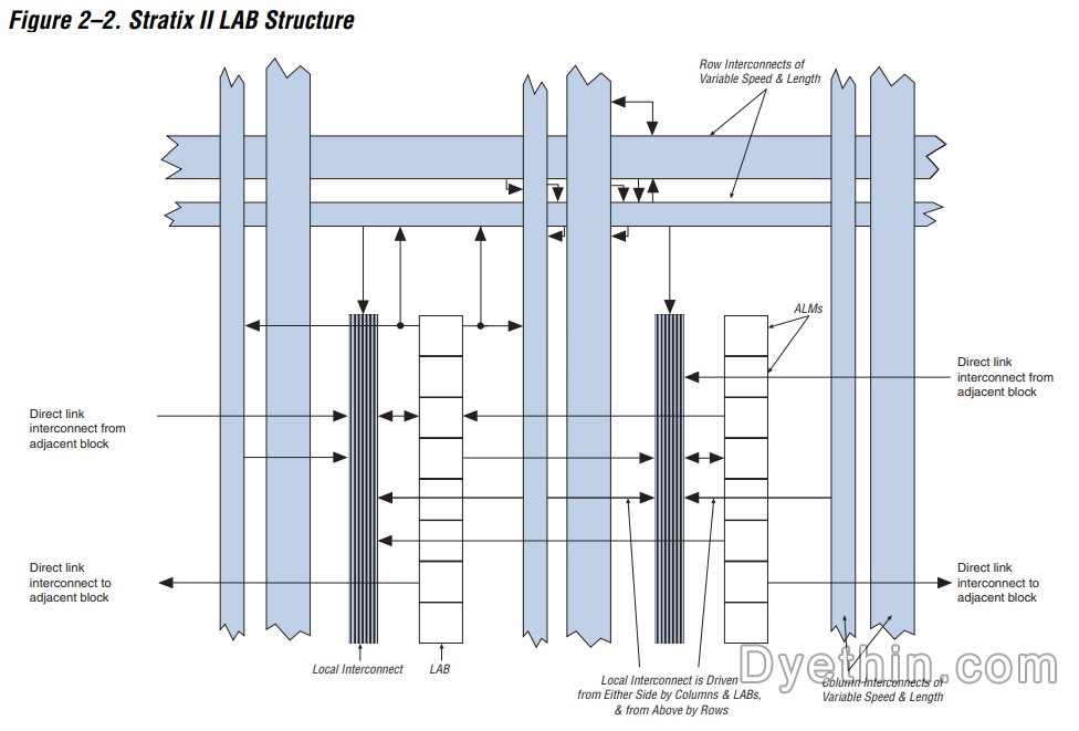
Intel/Altera FPGA
Intel/Altera FPGA consists of: ALMs, LEs, RAM, DSP Blocks, Multipliers, PLLs, etc.
Intel/Altera's programmable logic unit is usually called LE (Logic Element, logic unit) and consists of a Register and a LUT. Then 10 LEs are organically combined to form a larger logical functional unit - Logic Array Block (LAB). LAB also includes carry chains between LEs, LAB control signals, LUT cascade chains, and local interactions. Wiring resources, register cascade chains and other wiring and control resources.
Xilinx FPGA
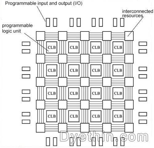
Xilinx FPGA composition: CLB (Configable Logic Block) includes Slices and DRAM.
CLB is composed of Slices. Each Slices is basically composed of LUT, carry chain, MUX and register.
Xilinx's programmable logic unit is called Slice and consists of upper and lower parts. Each part consists of a Register and a LUT, called LC (LogicCell, logic unit). There is also some shared logic between the two LCs. Cooperation and cascading between LCs can be completed.
Lattice FPGA
The main programmable logic unit composed of Lattice is called PFU (ProgrammableFuncTIonUnit), which is composed of 8 LUTs and 8~9 Registers.
LUT (look up table) look up table
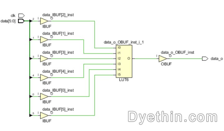
In FPGA, LUTs are mainly used to replace gate circuits. Write the code below to see the synthesized schematic diagram.
(1) If the logical expression is "6-bit input and 1-bit output", the synthesized result is a LUT6.
module lut_test(
input clk,
input [5:0] data
output data_o
);
assign data_o = data[0]&data[1]&data[2]&data[3]&data[4]&data[5];
endmodule
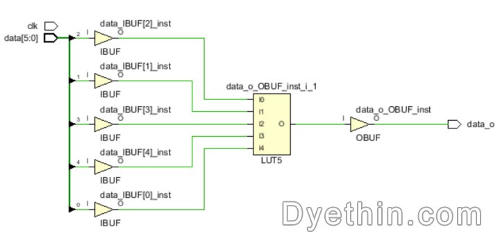
(2) If the logical expression is "within 5 bits input and 1 bit output", the result after synthesis is a LUT5.
module lut_test(
input clk,
input [5:0] data
output data_o
);
assign data_o = ((data[0]&data[1])^data[2]|data[3]&data[4]);
endmodule
MUX (Multiple Data Selector)
Take the four-select-one data selector (MUX4_1) as an example. MUX4_1 indicates that there are 4-bit data inputs (D0-D3) and 1-bit data output (Q). The address code is used to select the output.
module lut_test(
input clk,
input [1:0] addr,
input [3:0] data,
output reg data_o
);
always @(*) begin
case(addr)
'd0 : data_o = data[0];
'd1 : data_o = data[1];
'd2 : data_o = data[2];
'd3 : data_o = data[3];
endcase
end
endmodule
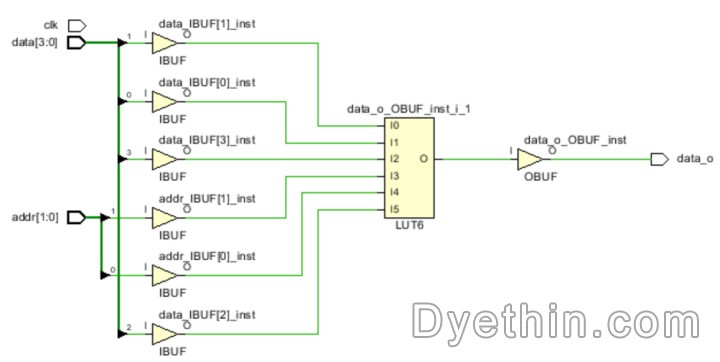
As can be seen from the figure, MUX4_1 is essentially a LUT6, except that it connects the 2-bit address input and the 4-bit data input to the input of LUT6.
Carry chain (half adder, full adder, multi-bit adder)
(1) Half adder
Two input data bits (A, B) are added and a result bit (S) and carry (C) are output. An adder circuit without carry input is called a half adder.
(2) Full adder
Two input data bits (A, B) and the input low-bit carry are added, and a result bit (S) and carry (C) are output, which is called a full adder.
(3) Multi-bit adder
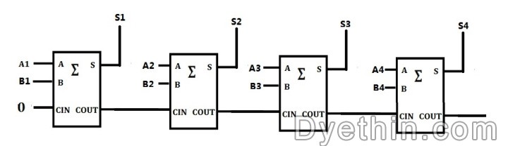
The lowest bit is a half adder, or a full adder with the low carry input set to 0. Then it can be cascaded with a full adder to make a multi-bit adder.
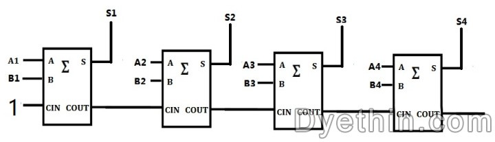
Set the low-order bit of the first full adder to 1, and the other three full adder cascades will become 4-bit subtractors.
Registers, Latches, and CLBs
Storage unit and CLB
(1) Trigger
By detecting the clock edge (rising edge, falling edge), the input is given to the output. A flip-flop is the basic unit of a computer memory device. A flip-flop can store one bit of binary code. A flip-flop can form a 1-bit register. Multiple flip-flops can form a multi-bit register.
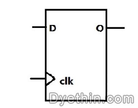
(2) Latch
The stored output state is changed by detecting the enable signal level (high level, low level). Because the latch does not require a clock, it is not a sequential component. It has no glitch filtering function, is very sensitive, and is prone to problems. In many cases, its use should be avoided.
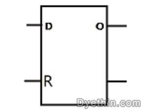
Note: In order to prevent the generation of latches, the judgment statement must be complete in combinational logic. For example, if statements must have else, case statements plus default, but sequential logic does not need to consider this issue.
(3) Storage unit
Taking the xilinx 7 series as an example, the main storage unit is the programmable logic block CLB. It has two SLICEs, each of which has 8 storage units. This storage unit is actually composed of 4 flip-flops FF and 4 flip-flops FF or latches).
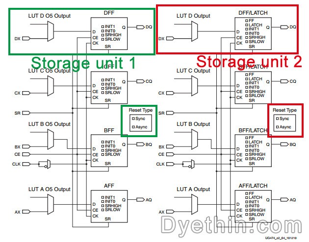
As shown in the figure above, the 4 storage cells on the left can only be used as flip-flops, but the 4 storage cells on the right can be used as flip-flops or latches.
Embedded RAM and DSP
Embedded RAM
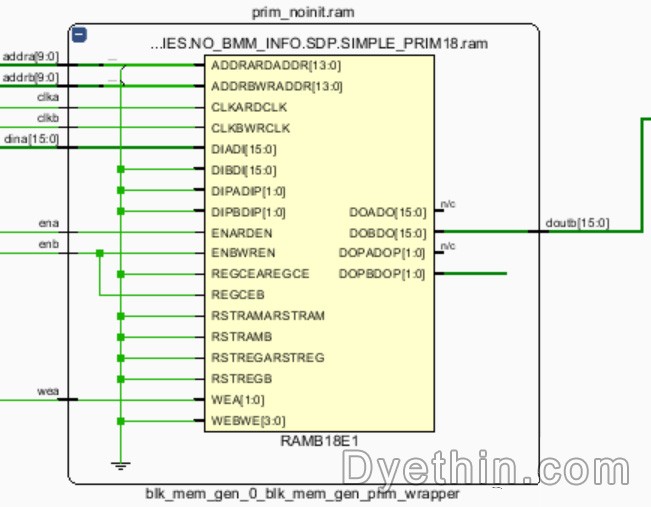
The embedded RAM blocks of FPGA include BLOCK RAM and ULTRA RAM, which can be flexibly configured into common memory structures such as ROM, single-port RAM, dual-port RAM, pseudo-dual-port RAM, content address memory CAM, and FIFO.
The RAM block sizes commonly used by Xilinx are 4Kbit and 18Kbit, the RAM block size commonly used by lattice is 9Kbit, and the RAM blocks commonly used by Altera are M9KRAM (9Kbit) and M-144K (144Kbit).
Taking xilinx dual-port IP as an example, after compilation, it is as shown in the figure below
DSP48E1
The basic structure diagram of dsp48E1 is as follows:

(1) A pre-adder (adder) implements the addition of A (maximum bit width 30) and D (maximum bit width 25). The maximum bit width of the output result is 25. This pre-adder is not used. You can choose to bypass it.
(2) A 25x18 multiplier, the two multipliers are B (maximum bit width 18 bits), and the lower 25 bits of the result after adding A and D. The output result is 48 (the upper 5 bits are sign extension bits, The lower 43 bits are data bits)
(3) This function has many functions. It can be used as an addition (subtraction) device, accumulation (subtraction) device, logical operation (AND or NOT), and the maximum output bit width is 48 data bits + 4 carry bits.
(4) A pattern detector, which mainly implements masked data comparison, upper and lower overflow detection, and resets the result when a certain number is reached.
(5) A data selector, its two data input terminals are C and P (maximum bit width 48), which can determine whether DSP48E1 performs ordinary addition or accumulation function.
Routing, PLL, and I/O Resources
Cabling resources
Wiring resources are similar to the wiring resources when drawing a PCB board. They are designed to allow resources such as logic resource blocks, clock processing units, BLOCK RAM, DSP and interface modules located at different locations in the FPGA to communicate with each other, thereby coordinating and cooperating to complete the required tasks. Function, length and process of the connection determine the driving ability and transmission speed of the signal on the connection.
There are mainly three types of wiring resources available:
(1) Global dedicated wiring resources: used to complete the wiring of the global clock and global reset/set within the device.
(2) Long-term resources: Complete the wiring of some high-speed signals and some second global clock signals between device banks.
(3) Short-term resources: Complete the logical interconnection and wiring between basic logic units.
(4) Other resources: There are also various wiring resources and control signal lines such as dedicated clocks and resets inside the basic logic unit.
Bottom-level embedded functional units
Highly versatile embedded function modules, such as PLL, DLL, DSP and CPU, etc.
Inter/Altera chips integrate PLL, Xilinx chips mainly integrate DLL, and Lattice's new FPGA integrates both PLL and DLL to meet different needs.
The PLL module of the Inter/Altera chip is divided into enhanced PLL (EnhancedPLL) and fast PLL (FastPLL).
The module name of Xilinx chip DLL is CLKDLL, and the enhanced module of CLKDLL in high-end FPGA is DCM (Digital Clock Management Module).
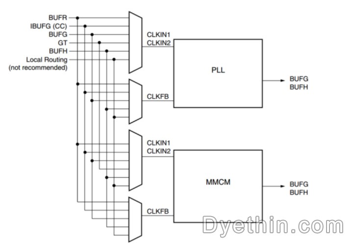
The full name of PLL is Phase Locked Loop, which is a phase-locked loop that electronic engineers often talk about. It is also a feedback control circuit that can perform system-level clock management and offset control on the clock network to achieve clock multiplication and division. frequency, phase offset and programmable duty cycle.
User programmable I/O
User programmable I/Os (User I/Os, also known as IOE) are distributed around the entire chip, as shown in the figure below.
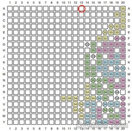
Taking xilinx as an example, the usual function naming format of xilinx is: IO_LXXY#/IO_XX.
IO stands for user IO;
L represents the difference, XX represents the unique identification number under the current BANK, Y=[P|N] represents the P or N of the LVDS signal;
# represents the Bank number.
For example, IO_L13P_T2_MRCC_12 means that this is a user IO, a differential signal, the 13th pair of differential P ports of BANK12, and also a global clock network input pin (MRCC is a global clock network)
In addition to the user IO of the FPGA, there are many other functional IOs, such as download interface, mode selection interface, MRCC, power pins, etc.

Articles you may also like
CR2025 Battery: Equivalent, Specifications and Replacements
Understanding Toggle Switches: A Comprehensive Guide
CR1616 Battery Equivalent: Best Replacement Guide
CR1632 vs CR2032: Are CR1632 and CR2032 battery equivalent?

-
-
-
-
-
-
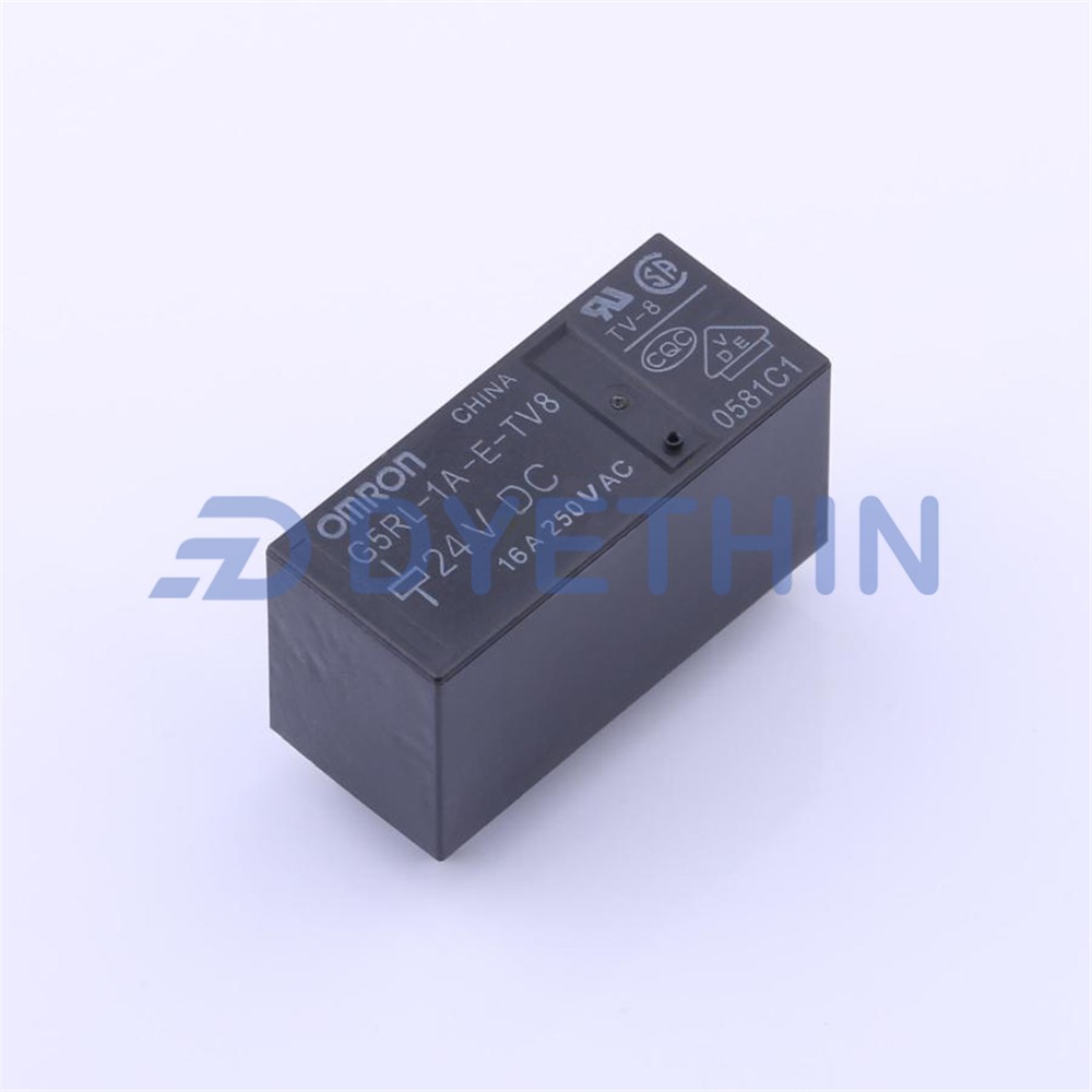
omron-electronics-inc-emc-div
General Purpose Relays SPST-NO (1 Form A) 12 A 24VDC
-
-
-