













- Strona główna
- Blogs
- Basic knowledge
- What are the causes of PCB soldering defects?
What are the causes of PCB soldering defects?
Here, a total of 25 types of PCB welding defects are summarized, along with analysis of the causes of welding defects, preventive measures, and solutions.
There are mainly 13 types of wave soldering defects and 12 types of PCB soldering defects and preventive measures.
What is wave soldering?
The basic principle of wave soldering is quite simple. After placing the component on the PCB and inserting its leads into holes drilled or punched through the PCB ("through holes"), place the component on the conveyor belt. The conveyor belt moves the components through a liquid solder tank (commonly referred to as a "tank"). The solder is pumped through the chimney, forming a ridge that flows through the bottom of the PCB, forming a connection between the component leads and the PCB circuit.
Although the principle is simple, this process requires controlling many variables, each of which may lead to serious defects.
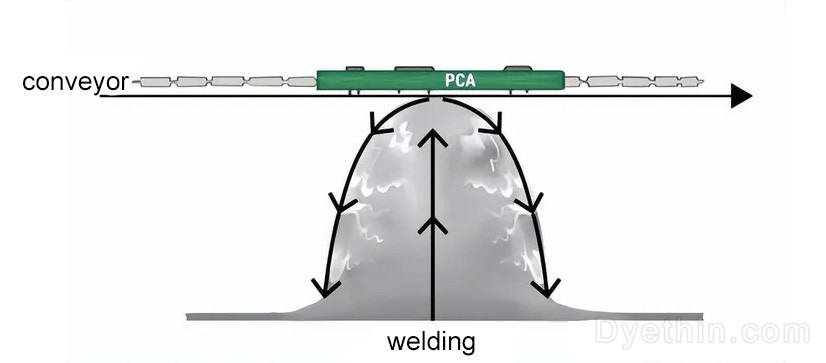
Schematic diagram of wave soldering
Wave soldering has been used to weld surface mount devices ("SMD"), but this technology is most suitable for "through hole" components (components with leads inserted into circuit board drilled holes).
Wave soldering process
When designing a PCB for wave soldering, PCB Layout engineers need to pay attention to three issues:
Pad spacing: If the pads to be welded are too close together, liquid solder will flow between them, resulting in not only a short circuit between the two connected pads, but also a possible short circuit across the entire PCB.
Solder resistance layer: PCB is usually coated with a solder resistance layer. But it is still necessary to carefully check the solder mask layer to prevent some unnecessary errors.
Soldering flux: Once the PCB pad spacing and solder mask to be welded are checked, soldering flux needs to be used. Flux helps to ensure that the area of the circuit board that needs to be soldered is clean and free of oxidation.
Wave soldering defects and preventive measures
1. Pores and pinholes
1) Pinholes and pores
Pinholes or air holes are mainly caused by deflation during the welding process of printed circuit boards. The formation of pins and pores during wave soldering is usually related to the thickness of copper plating.
During the welding operation, the moisture inside the circuit board is heated into gas, and when it is still in a molten state, it will escape through the solder. When the solder joint solidifies, gas continues to escape, forming voids. The circuit will temporarily conduct, but it is easy to cause long-term poor continuity.
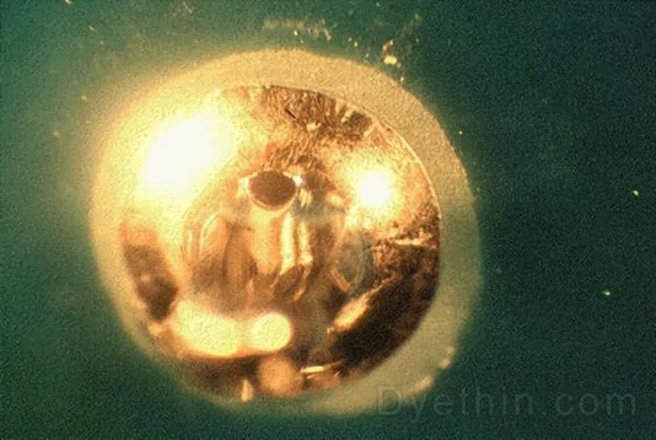
pore
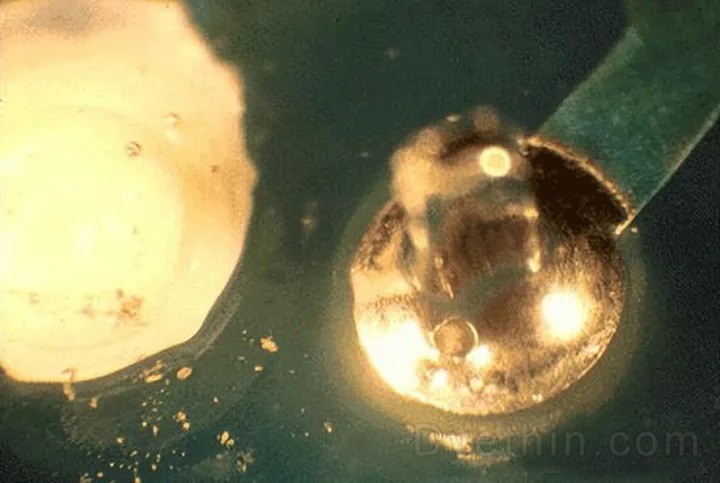
pinhole
2) Cause of occurrence
PCB top temperature too low
Excessive water accumulation in the circuit board may attempt to escape through a thin copper plating layer.
Failure to orient similar types of components in the same direction can lead to poor copper plating processes.
The ratio of leads to holes is either too small or too large.
3) Solution
Improve the quality of the circuit board by plating at least 25um of copper in the through-hole.
Baking is usually used to eliminate the problem of air release by drying the board. The baking board will carry water out of the board, but it cannot solve the root cause of the problem.
4) Preventive measures
Verify the temperature of the top PCB, verify the deposition of flux and the required preheating temperature, check the moisture in the laminate, and perform pre baking if necessary, but check the hole plating.
2. Ball joint/excess fillet
Solder joints on chip components that exceed the height of parts with convex curved surfaces are called spherical or excessively rounded. It is caused during the separation of the plate and welding wave, and is more common in nitrogen welding.
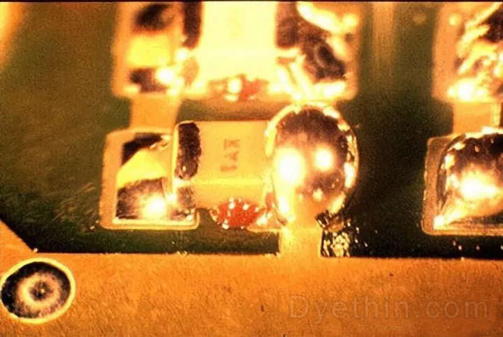
SMD spherical joint/excess fillet
3. Crack joint
Solder joint cracking on plated-through connectors is uncommon.
1) In the picture below, the solder joint is on a single panel and the connector has failed due to the expansion and contraction of the wires in the connector.
In this case, the fault lies with the initial design, as the board does not meet the requirements of its operating environment. Single-sided joints can fail during assembly due to improper handling, but in this case the joint surface will show lines of stress created during repeated movements.
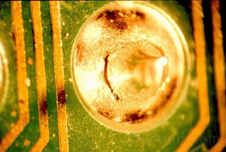
The stress line here indicates that this type of crack on the single panel is caused by repeated motion during the machining process
2) The following figure shows the cracks around the bottom of the rounded corner that have separated from the copper solder pad, which is likely related to the basic solderability of the circuit board.
There was no wetting between the solder and the surface of the solder pad, resulting in joint failure. Due to the thermal expansion of the joint, joint cracking usually occurs, which is related to the original design of the product.
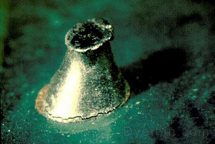
Lack of wetting between the solder and pad surface leads to cracks at the bottom of the fillet
4. Tombstone
The lifted component, also known as a tombstone, is a component that is lifted from the board during the welding process.
1) In the case shown below, due to the thermal demand for the leads, the component is lifted. Simply increasing the soaking time in waves can solve this problem.
The reason for the component to tilt is:
Incorrect lead length caused the lead to collide with the solder groove and lift during the wave crest.
The bending of circuit boards is common in large connectors, IC sockets, or large IC packages. Basically, the circuit board will bend while the components remain stationary.
Turbulent waves used for surface mount applications can enhance lightweight components.
Components with different thermal requirements or solderability of leads may also cause uplift during wave contact. Although not related to waves, vacuum formed shrink packaging may cause uplift during wave contact.
Shrinkage packaging is sometimes used to fix components to the surface of a circuit board for wire cutting, which can be pulled under the wire, causing the component to lift during wave contact.
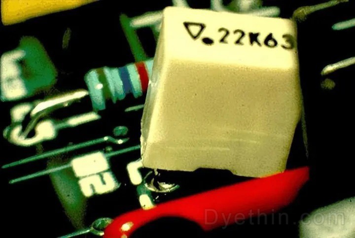
Increasing the soaking time in waves can prevent the occurrence of this problem
2) In the case shown below, the part was not inserted correctly before entering the welding process.
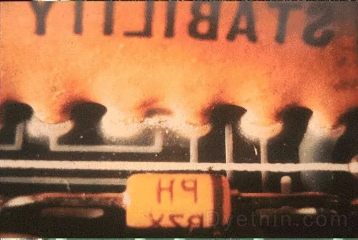
This defect originates from the assembly process, where the parts were inserted incorrectly
3) Solution
To fix the incorrect lead length, check the used leads. If the leads are too long, hitting the solder slot will push them out. It is possible to increase the immersion time in the wave, which should reduce the thermal demand for the leads and allow them to stabilize.
To correct PCB bending or other bending related issues, carefully check the PCB type and its heat capacity difference. Board bending is common on large connectors and large IC packages or sockets. PCB (such as plastic) that has been bent from the beginning should not undergo wave soldering, as wave soldering can cause the plastic to bend and lift the component off the circuit board.
Finally, the heat capacity difference of the circuit board was checked, and the heat capacity difference of all components was checked. Components with different temperature requirements or wire solderability temperatures will also increase when exposed to waves, as some components will be soldered down, while excessive heat will push other components apart.
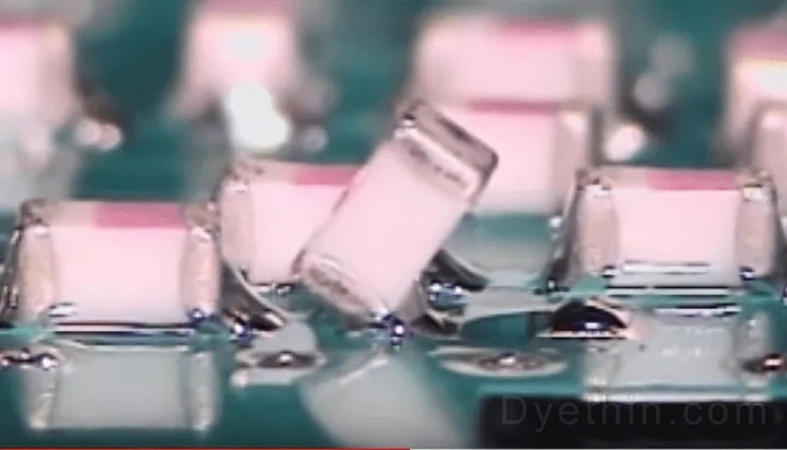
Mounted tombstone
5. Solder resist residue
Due to the reduced use of cleaning agents in industry, visible flux residues on boards are more common.
In the figure below, the residue is either the result of the flux formulation or due to poor process conditions. Many cleaning free materials rely on the correct preheating temperature to help minimize residue left on the board.
Wave contact time may also affect the residue left on the board, and discussions with flux suppliers should provide correct process parameters.
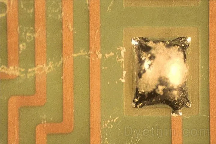
The flux residue here may be caused by the formula of the flux or poor process conditions
6. Ribbon and solder splatter
1) Ribbon and solder splatter
The specific details are shown in the following two figures: these solder sheets adhere to the solder mask layer with messy splashes, presenting a spider web like appearance.
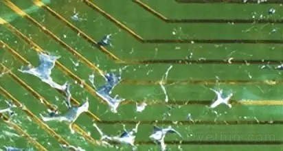
Welding spatter during wiring
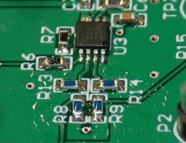
Welding spatter around surface mount components
2) Cause
Insufficient use of flux or contamination on the surface of the plate during wave soldering.
Unstable soldering iron temperature can also cause this phenomenon, and solder splashing/webbing may cause short circuits.
3) Solution
Easy to remove with a knife tip or tweezers.
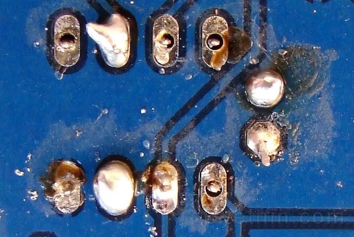
Ribbon and solder splatter
4) Preventive measures
If it is because there is too much rosin type flux in the solder wire, it is recommended to reduce the amount of solder wire additives.
If it is due to unstable soldering iron temperature, it is recommended to use a constant temperature soldering iron table.
Keep the surface of the wooden board clean.
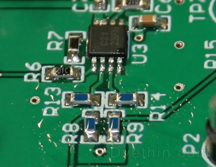
Webbing and solder spatter
7. Incomplete joint
Incomplete welding corners are often seen on single sided boards after wave soldering.
1) In the figure below, the lead hole ratio is too large, resulting in difficulty in welding. There are also signs of resin coating on the edges of the solder pads.
The example shown in the following figure is the result of burrs on copper solder pads. During the drilling or stamping process, the copper on the surface of the circuit board may deviate in certain areas, resulting in difficulty in welding. If resin is applied to the edge of the solder pad, the same situation will occur.

Incomplete joint
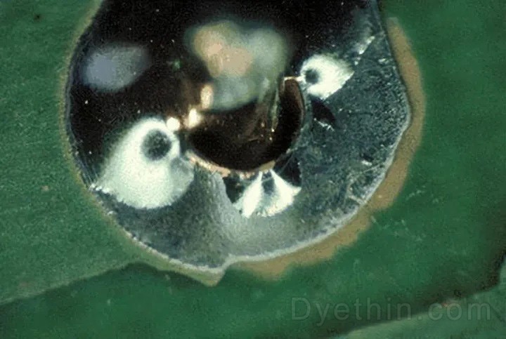
Burrs on copper solder pads
2) Cause
Poor hole to lead ratio
Steep transmission angle
Excessive wave temperature
Contamination at the edge of the solder pad
3) Preventive measures
It is possible to improve welding performance by reducing the angle of the conveyor belt from 6 ° to 4 °. This will reduce the drainage performance of waves, but it will lead to the occurrence of short circuits.
Reduce wave temperature.
The ratio of holes to leads is usually the lead diameter plus 0.010 ".
8. Inconsistent or poor hole filling
1) The solder did not fully fill the electroplating through-hole shown in the repair diagram. This is due to low preheating setting or poor application of flux. In both cases, checking the process parameters should eliminate the problem.
This is a common problem when switching from foam flux to spray flux device; This is because the flux is difficult to penetrate into the through-hole.
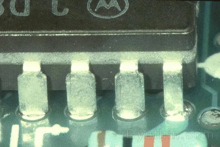
Solder has not completely filled the electroplated through hole here
2) In the following figure, the poor hole filling is due to the preheating setting. The solder wetted the lead of the device, but failed to wet the surface of the through hole.
The top temperature of the printed board before wave contact should be 100-110 ° C. This generally applies to double-sided and multilayer boards. The single panel will be processed at a slightly lower temperature because solder penetration is not required.
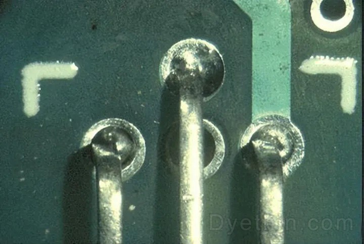
Solder failed to wet the through-hole surface here
3) The solder does not completely fill the electroplated through hole in the following figure. This may be due to the preheating operation set too low or poor flux application. In both cases, inspection of process parameters should eliminate the problem.
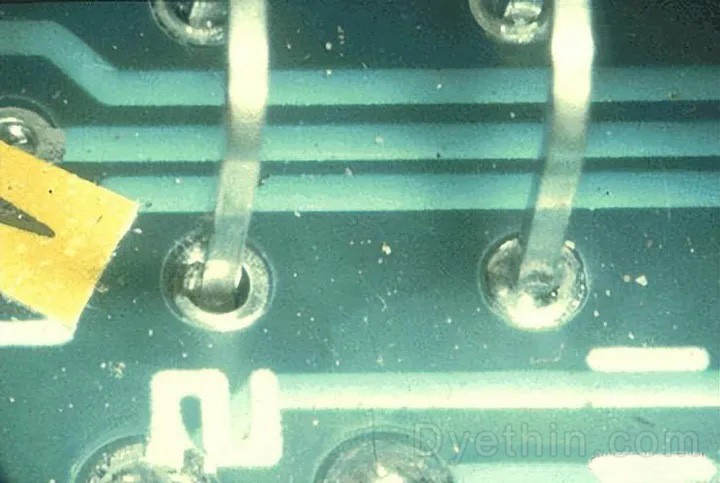
Solder does not completely fill the electroplated through hole on the left
4) In the following figure, one hole is filled and the second hole is not filled, which indicates that the problem is unlikely to be the problem of the printed board. Here, the solder has solidified on a hole due to the thermal demand of the component. This problem should be solved simply by increasing preheating or by increasing wave contact time.
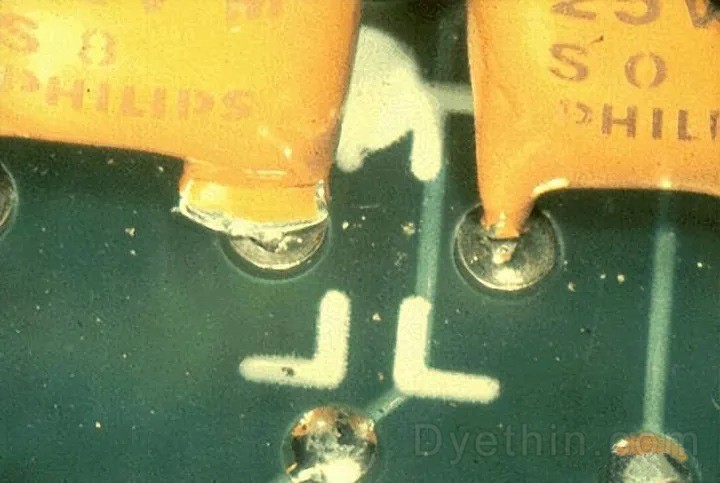
A hole has been filled; The other one didn't
5) In the following figure, there is no indication that there is solder in the through hole or through hole. Due to the wave height, finger damage or the tray not being maintained, the wooden board is likely to fail to contact the wave, and the circuit board may also be incorrectly loaded into the system.
The quality of through-hole plating may be the cause of the problem, but this is unlikely to happen.
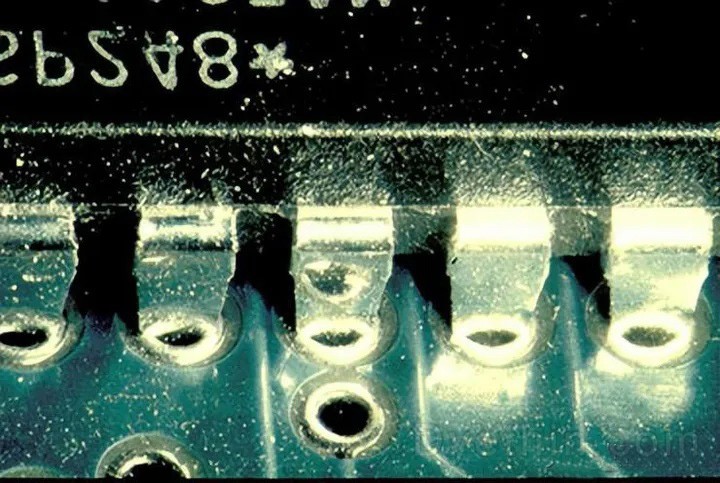
This plate is likely to fail to contact the waves
6) The example of poor hole filling in the following figure is very unique, because the problem is caused by the legend on the printed board. Careful inspection revealed that the poor design rules made the legend contaminate the top of the plated through-hole. Solder fails to rise in the hole or soak the pad surface. In this case, the legend has no benefit and new design rules need to be applied.
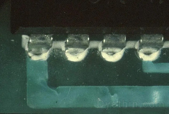
The legend on the PCB contaminates the top of the electroplated through hole
7) The following figure shows the poor wettability of the pad surface, which may be due to the thickness of the tin / lead coating. Solder leveling usually leaves a thin deposit on the surface of the pad and the edge of the hole. This defect is often referred to as the weak knee effect, in which the solder cannot wet on the knee of the hole and the pad.
Poor hole filling may also be due to the setting of preheating operation too low or poor flux application.
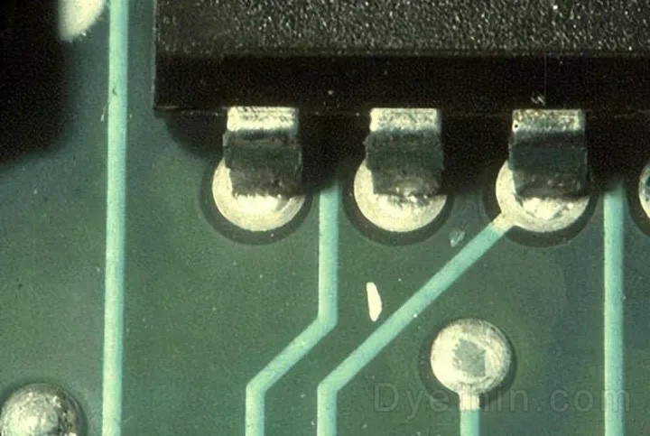
Example of "weak knee" effect
Preventive measures:
Verify flux deposition, verify preheating temperature, check wave height, check the aspect ratio of lead to hole, verify internal ground plane
9. Combined pollution
The top of the electroplated through hole in the following figure has been contaminated during the welding operation. The temperature causes the coating on the resistance network to soften and contaminate the surface of the circuit board.
During preheating, the top plate temperature is usually 100-110 ° C, which may reach more than 190 ° C when exposed to waves. If the normal process conditions are maintained, the component should not cause this problem, and the compatibility of the component welding process should be re evaluated.
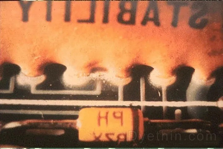
Combined pollution
10. The solder pad is lifted
Raised pads are rarely seen on plated through-hole boards, but may appear on single boards during assembly.
1) The picture below occurs directly when processing components after wave soldering. Copper foil adhesion decreases as surface temperature increases, so after soldering the copper foil adhesion will be very low and any handling or force applied to the component may cause the pad to lift.
Care is required when lifting boards from conveyors or pallets, as operators often use large components as handles.
During processing, this raised pad occurred after wave soldering
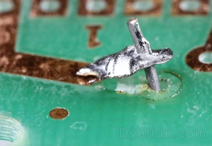
Raised pad
Reasons for pad lifting may include:
Overmachine the pad joint where the layer between copper and circuit board is damaged.
A circuit board designed with a thin copper layer.
Through hole component leads are not coated with a uniform layer of copper.
2) Solution
The simplest repair is to fold the lead onto the copper trace that is still connected and weld it, as shown in the following figure. If there is a solder mask, it needs to be carefully scraped off to expose the bare copper.
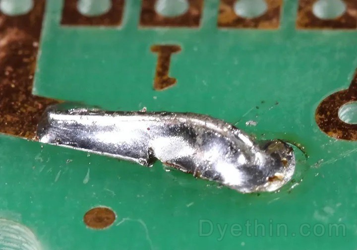
Repaired pad
The other alternative is to follow the trace to the next through hole and run the jumper here.
Or, in the worst case, follow the wiring to the nearest component and weld the jumper to the pin of the component.
11. Resist on PCB
The following figure shows a very obvious example, that is, after welding, the resist is stripped from the surface of the circuit board. Quite simply, this is caused by the incorrect specification of the printed circuit board.
Tin / lead should not be used as a resist on professional circuit boards. When tin / lead enters the liquid phase, it will expand and may cause the loss of adhesion between solder and resist.
If the resist is brittle or thin, it will separate as shown in the following figure. If the thickness of the coating is less than 3-5 µ m, tin / lead can be used because there is little movement during wave soldering or reflow soldering.
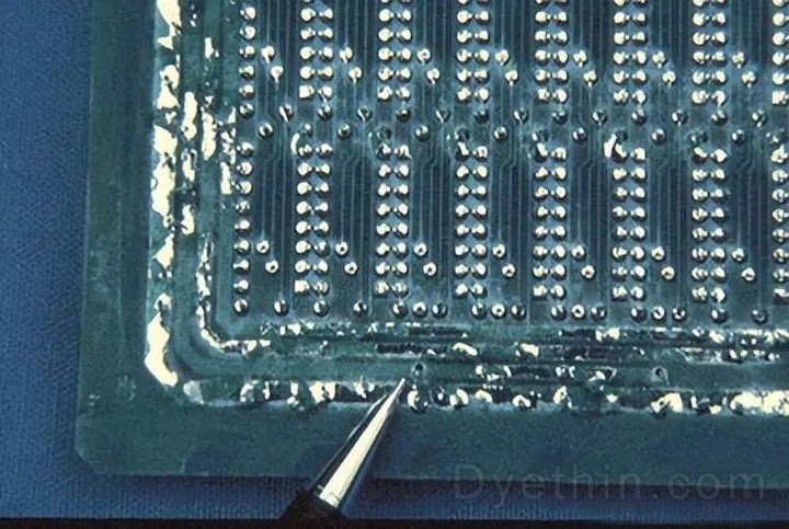
Resist on PCB
12. Pad contamination
1) The solder joints shown in the figure below are good, but the solder amount is reduced due to the solder resist on the pad. The resist on the board is directly related to the poor design rules used on this printed board.
The correct design rule for the resist aperture is a 0.002-0.003 "ring around the pad.
The following example is designed to have a resist aperture smaller than the pad size. It is worth pointing out that during wave soldering, the resist on the pad may affect the appearance of the joint, but will not cause any reliability problems.
2) Solution
Use a reduced resist aperture to eliminate solder shorts.
If you don't want to change the design, use glue dots. Setting an additional glue point between the leads that are always short circuited will be a simple repair.
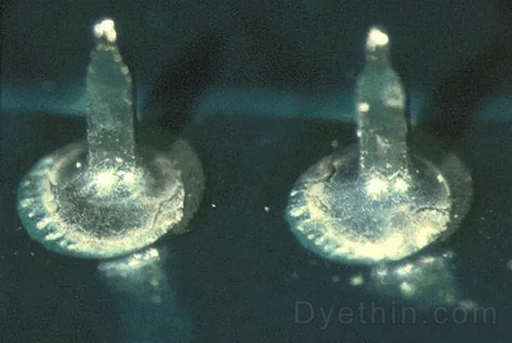
The hole diameter of the resist is smaller than the pad size
13. Cold joint
1) The following figure shows a block and matte cold joint. The surface of the cold joint appears dim, uneven and pitted.
The cold joint is the same as the faulty welding. It is difficult to fully expose in the production process. It often requires users to use it for a period of time, which may be days, months, or even years. This will not only have an extremely bad impact, but also cause extremely serious consequences. Due to the low strength of cold welding, the conductivity is not good.
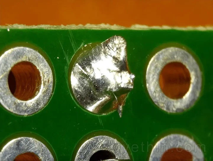
cold junction
2) Causes
Because the heat transferred to the joint is not enough to melt it completely.
The soldering iron or the connector itself may not have been given enough time to fully heat.
The soldering iron temperature may not be set high enough to melt the specific solder type being used (for example, lead-free solder has a higher melting temperature), or this may be the result of the design of the pad and the routing itself.
If a pad is directly connected to the ground plane without considering the heat dissipation, the heat of the soldering iron will be lost to the ground plane.
3) Solution
To repair the cold solder joint, simply reheat the joint with a hot soldering iron until the solder flows.
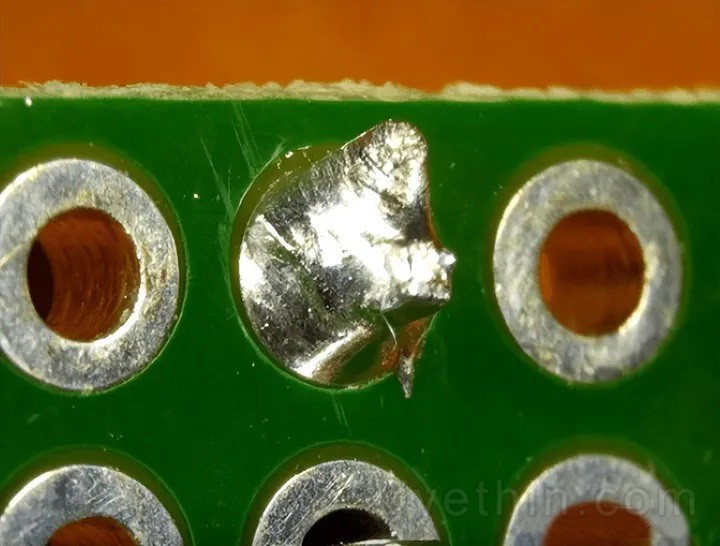
cold junction
14. solder bridge
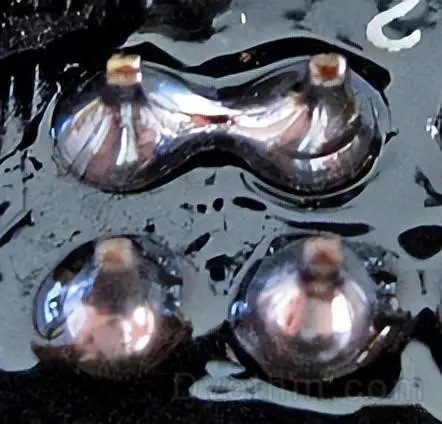
Solder bridge diagram
Solder bridging is the most common problem in the welding problems caused by small components. When two solder joints on the circuit board that should not be connected are inadvertently connected by solder during PCB welding, bridging will be formed. Depending on the circuit structure, various damages may be caused.
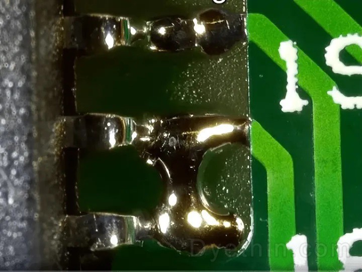
Solder bridge diagram
1) Possible causes:
Too much solder is used between joints
Too wide or too large soldering iron head
Protruding lead length is too long
Insufficient flux
Solder drag speed is too fast
Nozzle peeling movement
Improper exit angle of soldering iron
Design a PCB with poor weight distribution and large components on one side
There is not enough space left between the pad and the solder mask
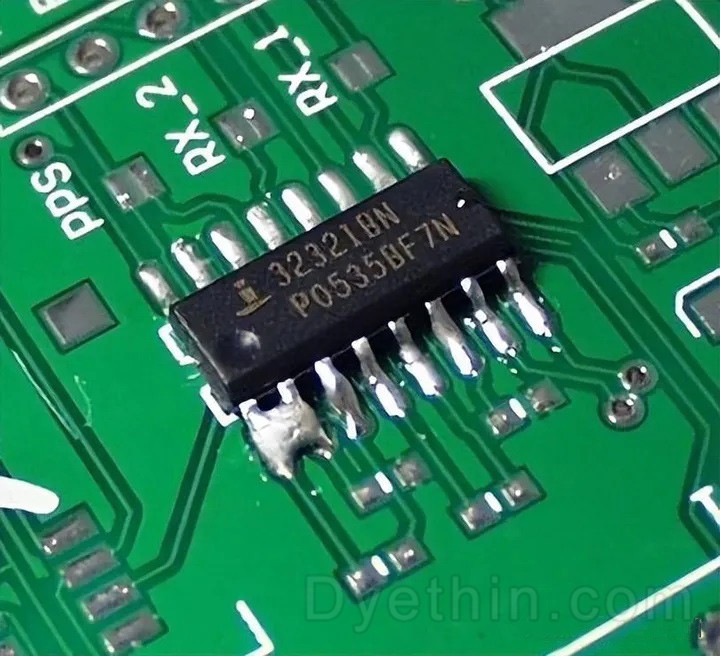
Solder bridge
2) Solution:
Sometimes the excess solder can be sucked off by dragging the tip of the hot soldering iron between two solder joints
If there is too much solder, solder cups or solder cores can help remove excess solder
3) Preventive measures:
Use the correct lead length
Set the correct hole size and pad diameter
Verify flux deposition
Reduce towing speed
Reprogram peel motion
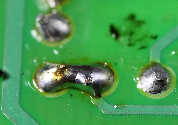
Solder bridge
15. Poor weldability and wettability
1) In the following figure, the solder did not wet the pin terminals, but wetted the through holes.
In this case, plating is a problem because brass pins are not properly copper plated before tin lead plating. Copper plating is very necessary to prevent the migration of zinc affecting the tin / lead surface.
In order to extend the solderability life by at least 0.002 µ m, there is at least 0.005 µ m tin / lead on copper.

Brass pins are not copper plated before Tin Lead Plating
2) In the following figure, the solder failed to wet the lead surface during wave contact.
This problem is caused by the edge solderability of the lead wire and the service life of the 10% solid flux used in production (the flux quality is too poor). The flux after grooving will decrease, and its performance will change even if the solid content remains unchanged. Generally speaking, the supplier of components only guarantees the welding of components for twelve months.
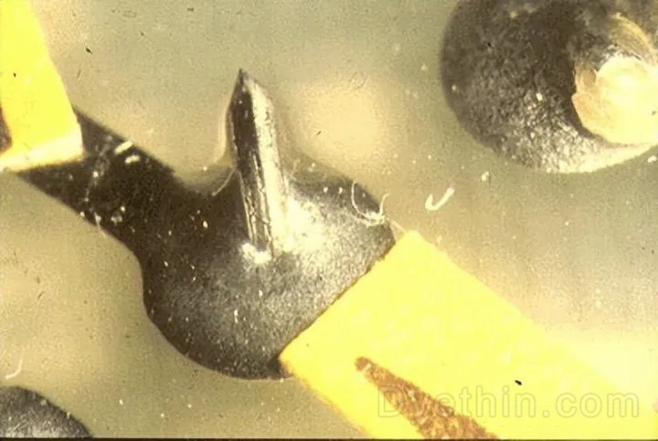
The deteriorated flux causes the solder to be unable to wet the surface of the lead wire
If the correct thickness of tin / lead is applied to the surface of the pad, poor solderability on the tin / lead plate is relatively rare. As a recommendation, a minimum thickness of 0.005 µ m should provide a weldable coating with a shelf life of more than 12 months. Only in this way can the surface be protected under normal conditions for several years and still have high weldability.
3) In the following figure, only part of the pad surface is wetted by solder, and neither the outer edge nor the inner edge is wetted by solder.
This is because the tin / lead on the surface of the circuit board is less than 0.002 µ m, and there is no reflux during the circuit board manufacturing process, so the shelf life of the product is short.
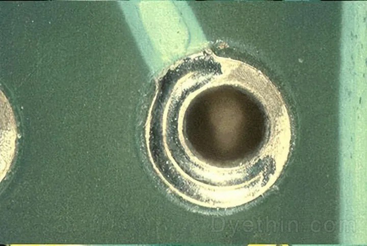
The through-hole pad surface is only partially wetted - the inner and outer edges fail to be wetted
4) In the following figure, the pad was not wetted during welding.
This is due to the poor solderability of the pad surface. The solderability of PCB should be tested, because the surface has been dewatered after welding, which may be related to PCB.

Defects are caused by poor solderability of the pad surface
5) In the following figure, only the corners of the pins are not wetted.
Poor solderability of pins may be due to poor plating or thin or long storage time. Solderability of tin / lead pins is usually a function of plating thickness or plating and substrate. In the case of brass pins, before applying tin / lead, the pins must first be plated with a 1-3 µ m copper layer; Otherwise, the zinc in brass will soon affect the weldability.
Weldability is also thickness dependent. If 0.005 µ m coating is present, it should provide a storage life of more than one year. This coating thickness applies to any substrate.
The example shown in the following figure is not an electroplating problem, but is caused by the printed board resin on the pin corner.
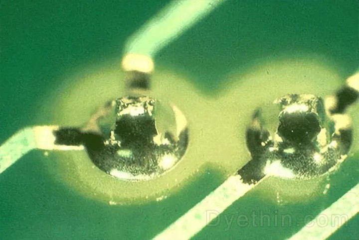
The corners of the pins are not wetted
6) The following figure clearly shows that the wettability of the component lead surface is poor, while the wettability of the pad on the PCB is good.
The possible reasons are: the components are stored for too long, or the tin / lead coating on the lead is too thin. The weldability of components shall be tested using wetting balance or immersion and inspection test.
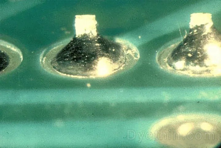
Good wettability of pads, poor wettability of component pins
7) The gold surface coating in the figure below is not wetted.
At first glance, it seems to be a skipped joint, but careful inspection is the solderability problem of PCB coating. It is usually caused by unbalanced electroless gold plating bath.

The gold surface coating was not wetted
8) Electroplated through holes are not completely wetted.
Due to poor soldering flux or preheating temperature, incomplete wetting or poor solder rise in electroplating through holes may occur. If it is not these two problems, it is the surface coating of PCB.
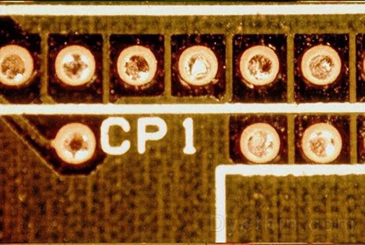
Incomplete wetting
9) The solder joints on the chip in the figure below are good, with rounded corners, but the leads are exposed.
The loss of coating may be due to the poor initial coating of the base lead frame prepared before tin / lead plating. Because the lead frame is polluted by mold overflow, the loss of coating is often seen at the interface between the lead and plastic.
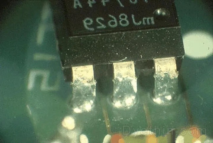
The solder joints on the chip are good, with rounded corners, but the leads are exposed
10) Brass pin failed to be wetted by solder
In fact, the tin plating has been separated from the substrate during the welding process. Before tin / lead plating, the brass pins should be coated with 1-2 µ m copper.
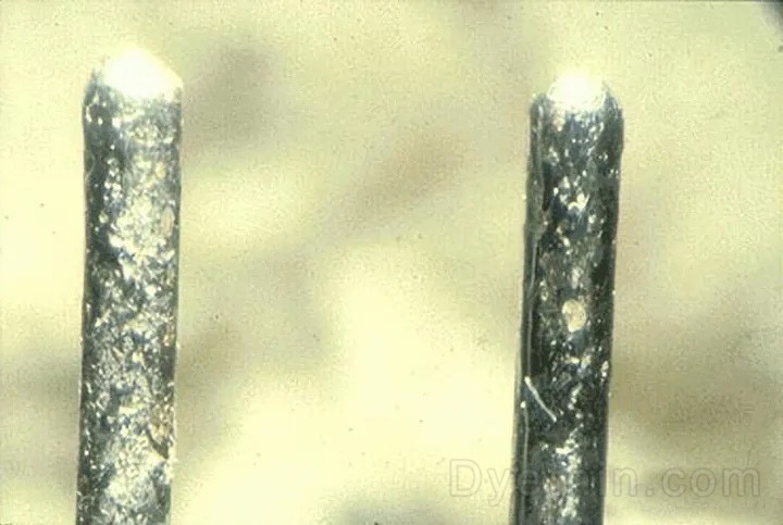
Brass pins should be plated with 1-2 µ m copper
11) The solderability of the pins is very poor - after the solder is immersed, the leads are not wetted.
The possible cause is poor thin tin / lead coating. A minimum of 5 µ m of coating should be used and provide a 12-month shelf life.
16. Poor penetration
1) In order to form solder joints on the top of the circuit board, the flux needs to be present in the electroplated through holes, and the temperature on the top of the circuit board must be at least 100-110 ° C.
If the products of PCB manufacturers are evaluated before use, there is usually no problem of through-hole plating.
Poor penetration is caused by insufficient flux application or preheating.
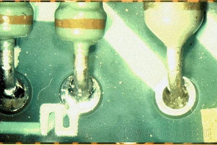
Poor penetration
2) In the following figure, the solder failed to fill the electroplated through hole on one side of the component. The solder wetted the PCB, but failed to completely wet the component lead.
This may be related to the flux, but if the fault is related to the process conditions, other positions on the PCB will certainly have similar problems.
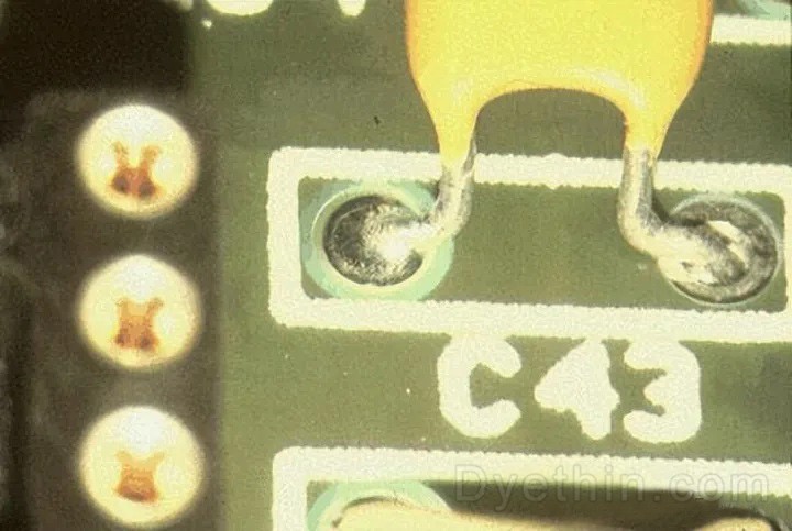
Poor permeability
17. Bleeding (degassing)
Degassing is a common problem associated with wave soldering and manual welding. Basically, when soldering a circuit board, any moisture on the circuit board close to the hole will be heated and turned into steam. If there is a thin coating or gap in the coating, the gas will pass through the coating hole wall. If there is solder in the hole, voids will be created when the solder solidifies.
As shown in the figure below, the gap may appear as a small hole on the surface of the joint or as a larger cavity. The correct copper plating thickness in the through-hole is the key, and the hole wall surface should have at least 25 µ m copper.

Voids caused by degassing
The most common causes or solutions:
When using flux without VOC, poor preheating process will lead to very fine spatter of welding balls.
The coating less than 20 μ m in the through-hole or the coating with very poor hole surface cannot cover the broken glass bundle that causes air bleeding.
18. Solder ball
1) The solder ball is obvious in the following figure, but it should be called solder attachment rather than solder ball.
Due to the failure of the resist coating, the solder wetted the track.
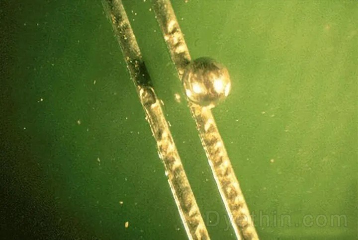
Manual removal of this solder attachment will damage the rail
The solder ball may be caused by poor process conditions, the flux will generate gas during wave contact, or excessive turbulence will cause splash when the solder flows back into the groove. During the welding process, due to the excessive degassing of PCB, solder balls may be ejected from the joint area.
2) The following figure shows that a solder ball is connected to the edge of the resist at the bottom of the circuit board, and must attach itself to the resist when it is separated from the pin.
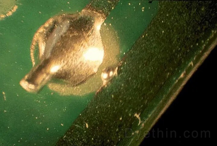
The solder ball must be attached to the resist when it is separated from the pin
3) In the following figure, the solder ball is connected to the edge of the resist at the bottom of the circuit board, and it must attach itself to the resist when it is separated from the pin.

Another solder ball attached to the edge of the resist
4) The welding ball in the following figure is on the line and cannot be removed casually.
This is caused by tin / lead extrusion below the solder mask, or simply adhesion. When tin / lead becomes liquid during reflow soldering or wave soldering, tin / lead will expand. Welding balls can be formed on the track. If the solder mask is thin, the solder may wet and leave a ball during wave contact.
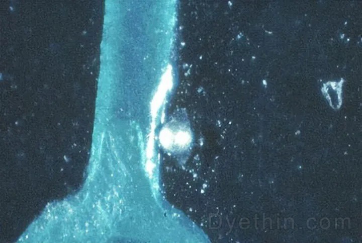
Solder on the resist may become wet and leave solder balls during wave contact
5) The position of welding balls is random.
This type of defect is usually caused by splash on the wave crest surface, which is related to the wave crest welding parameters. If the solder drops a distance from the printed board during wave separation, the solder may splash back from the molten pool. If the preheating setting is incorrect or the flux dosage increases, the evaporation of solvent in the flux may be affected. The use of glass panels on waves should cause air bleeding problems.
Ideally, when the glass touches waves, there should be a minimum of visible bubbles under the glass. The compatibility of the resist and flux should be checked. Generally, the mask is helpful for solder ball adhesion.

Solder balls are caused by spatter on the wave surface
19. Welding mark
Solder flags or spikes are caused by inconsistent flux application or poor control of wave soldering tin discharge.
Poor control of separation from welding wave is often a random fault, rather than on the same contact every time. During the separation from the wave, the solder should flow at the same speed and direction as the circuit board. Running a little faster usually does not lead to spikes, but running slowly or not flowing at all increases spikes.
1) Welding marks or spikes
Cause:
If the spike is always at the tip of the lead, it may be a solderability problem caused by the bare cut end.
If the lead is cut or cut by the supplier and stored for a long time, the bare end of the lead will be oxidized and difficult to be wetted by solder.
If the lead is wetted slowly, the drainage will also be very slow, so it will form a spike.
Solution
It can be eliminated by longer soaking time in waves or increasing preheating. During the preheating of the circuit board, the lead may not have the opportunity to absorb heat to overcome this heat load. As the leads of the components are separated from the waves, they will cool faster, leaving spikes or short circuits.
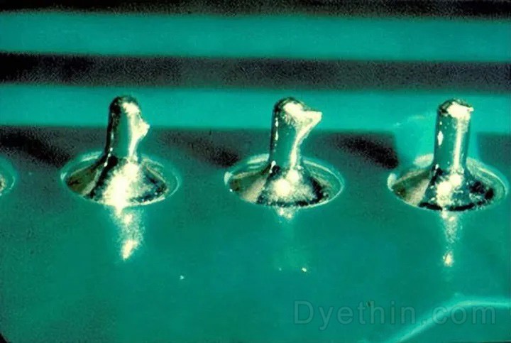
2) Solder marks may be caused by inconsistent flux
The length of the pin is also too long. The lead length shall not exceed 1.5-2.0mm below the board surface. If the component leads are dragged through the wave oxide layer instead of exiting from the clean surface, a short circuit may also occur during exiting from the back of the wave.
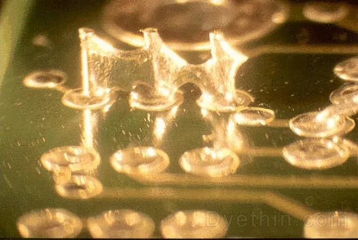
Inconsistent flux may cause these solder marks
20. Welding short circuit
Welding short circuit usually occurs in wave soldering process, which is due to the decreasing spacing of components used in manufacturing.
When the solder is not separated from two or more leads before the solder solidifies, a solder short circuit occurs. One way to reduce short circuit is to increase flux solids or quantity. Reducing the lead length and pad size will reduce the amount of solder held at the bottom of the board.
1) The following illustration shows a connector with a 0.025 "pitch.
The connector is improved by changing the design of the pad, and the length of the alternative pad is increased on the outlet side of the wave, which makes the actual spacing distance between adjacent terminals larger and reduces the short circuit.
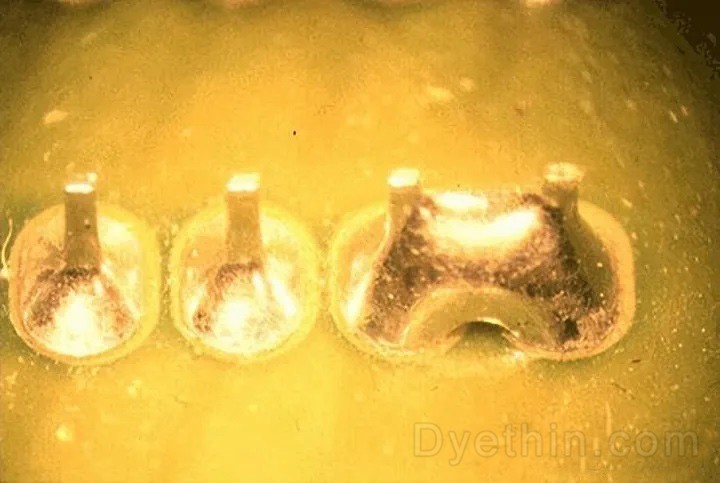
Short circuit of solder on connector with spacing of 0.025 "
2) In the following figure, the solder short circuit can be seen on the IC lead on the single-sided PCB.
During contact with waves, the pressure is so high that a short circuit occurs due to excessive penetration of solder. Due to the tolerances of these cheaper laminates, it is more likely to occur on single panels because the ratio of hole size to lead wire is usually greater.
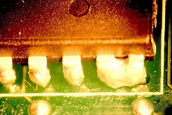
Rare solder short circuit on the top of printed board
3) Pin grid array (PGA) device is short circuited
Due to the close proximity and the number of pins, the separation of solder from the bottom of the plate is hindered. Short circuits may occur due to poor flux, incorrect preheating, or wave separation. All short circuits can be reduced by good design rules, while reducing pad size and component lead length.
In the figure, it is necessary to change the solid content of the flux while maintaining the cleaning free process. Due to the high mixing of circuit board and pin length, the use of hot-air knife failed to improve the process.

Short circuit on pin grid array
4) The pin length is correct to be 1-1.5mm, but the size of the surface pad is reduced, resulting in a short circuit.
With smaller pads, less solder remains on the circuit board, which shortens between the pins. A glue spot can be placed between the two pins.
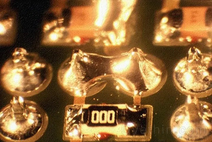
Smaller pads will reduce the possibility of this short circuit
5) SOIC device short circuit
Welding short circuit is common in SOIC devices. If the short circuit is in the middle of the line and the pad width is less than 0.022 ", it is a process problem. The flux is the first area to be checked, and then the contact time in the wave can be adjusted. This defect can be eliminated by frequently changing the angle of the conveyor belt.
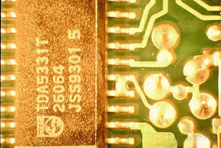
Welding short circuit on SOIC device
6) Welding short circuit at the top of QFP device pin
This defect is usually caused by incorrect preheating or too short time in the wave, which can be improved by increasing the solid of the flux. The thermal effect of the device may cool the solder, thereby slowing emissions.
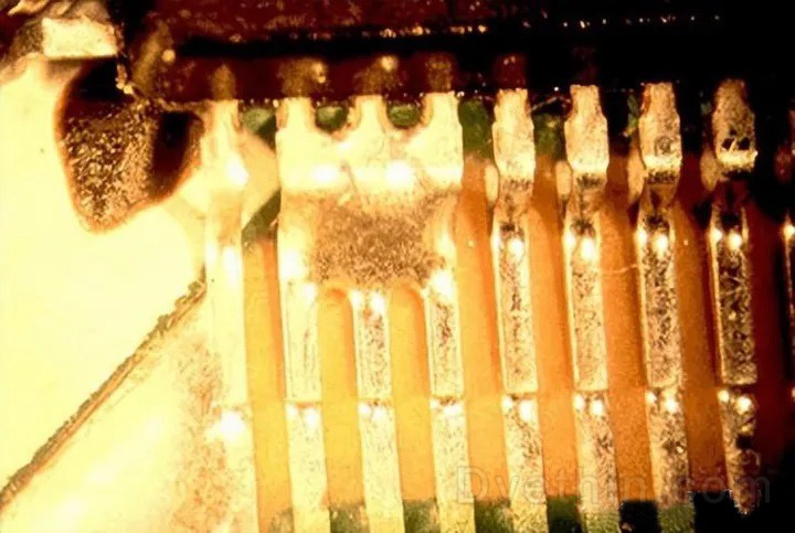
Short circuit at the top of pin on QFP
7) Welding short circuit caused by poor solderability of pins
In the following figure, due to the poor solderability of the exposed end of the lead, there are solder spikes at the end of the lead. If the terminal wetting is slow, the water drainage is usually slow, which will increase the incidence of solder short circuit.
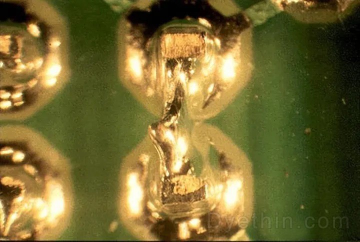
The poor solderability of the bare end leads to these solder spikes and subsequent short circuits
21. Missed welding
A surface mount joint that is not welded is called a leaky weld, in which the terminal does not have any solder. It is caused by incorrect chip wave height or gas of flux at the bottom of the circuit board.
1) Solder jump
In the following figure, the solder jumps due to the thickness of the solder mask. The solder resist or mask should be flush with or lower than the pad surface to obtain ideal assembly conditions. If the mask is very thick, it will form a cavity around the pad, and the flux vapor will be trapped in the cavity, forming bubbles. Solder cannot easily displace steam to form joints.
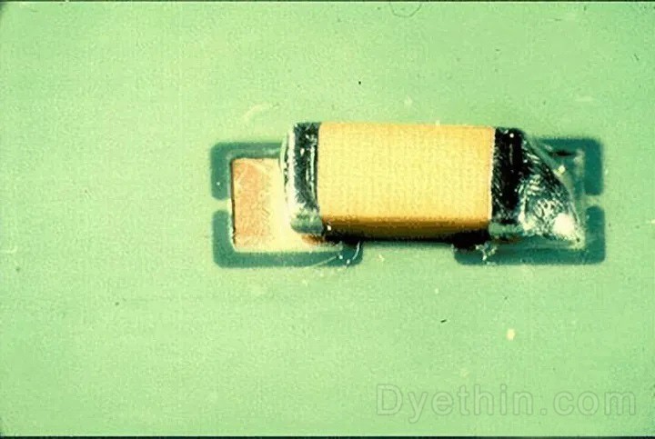
The thickness of solder resist layer is the reason for solder jumping
Check whether there is new solder coating on the pad or component terminal. Generally, the presence or absence of a new solder coating on the lead wire can indicate the root cause of the problem.
The most common reasons for skipping are the incorrect wave height of the chip, the gas generated by the solder under the surface of the circuit board or the excessive thickness of the resist. Each of these faults can be repaired.
2) The adhesive has contaminated the pad surface
Although there are no visible adhesive deposits, some adhesives will make the invisible film extravasate from the spot area during the curing process.
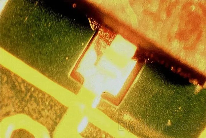
The adhesive contamination on the surface of the pad resulted in this missing solder
3) The case in the following figure is not welded
It is more likely that the circuit board is not correctly positioned in the finger conveyor or tray. The tray may be deformed or the clip does not keep the circuit board flat.
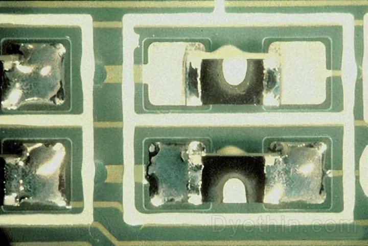
The circuit board may not be correctly placed on the finger conveyor or in the tray
22. Recessed joint
1) Solder joint depression caused by exhaust
The most common reason for the concave connector at the bottom of the circuit board is the exhaust of the printed circuit board. Just like the small sound (called pinhole or air hole) in the solder chip, it is another process indicator. If the copper plating thickness in the bore is kept at a minimum of 25 µ m, water will not be discharged through copper during welding.
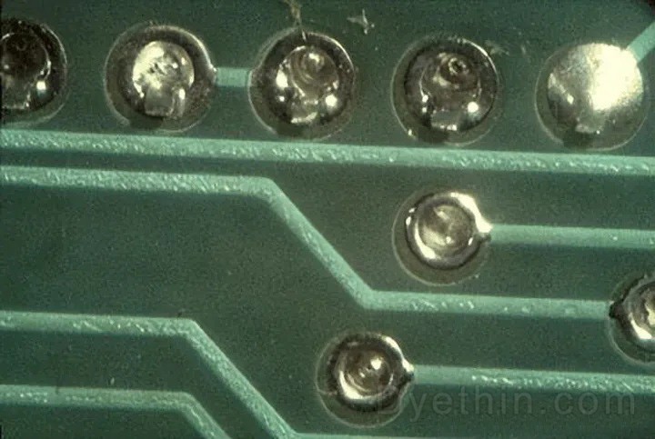
Solder joint depression caused by exhaust
At the top of the plate, dents or dented joints may occur due to the following reasons:
The ratio of holes sunk by solder due to its own weight to lead.
Some form of contamination or blockage does not allow the solder to rise in the hole.
Poor preheating or flux does not allow the solder to completely wet the plated through-hole.
2) The insulation of components interferes with the formation of welded joints
In the following figure, the insulation layer on the main body of the component is also found on the top of the lead wire, so it is difficult to form the welding head.
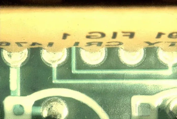
Welding head
The most common reason for concave joints is the ratio of holes to leads. If the hole is larger than the lead diameter, the solder will fall in or out of the hole.
If the solder does not return directly to the top of the circuit board, the recessed joint on the top of the circuit board may be caused by incorrect preheating or poor flux.
3) The adhesive contamination on the surface of the pad resulted in this missing solder
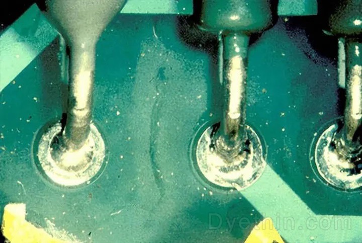
The adhesive contamination on the surface of the pad resulted in this missing solder
23. Solder mask discoloration
1) Dark stripes on solder mask after selective welding
The welding process or residence time may change when running thicker circuit boards.
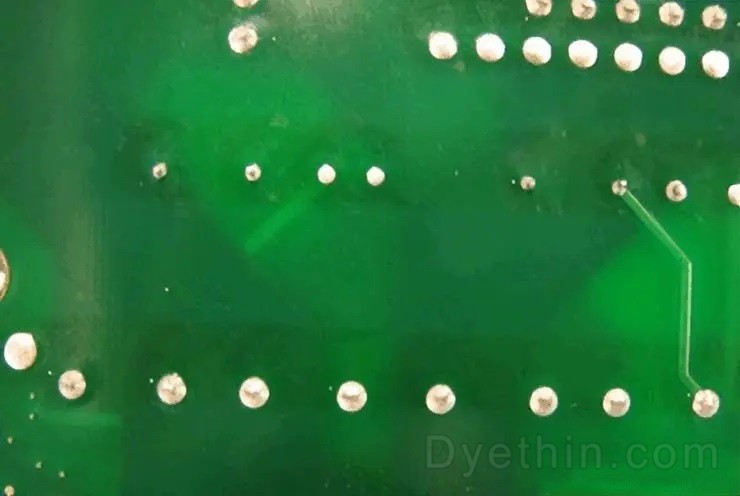
Dark stripes on solder mask after selective welding
The most common reasons for this include:
Use different flux, higher temperature, longer residence time or plate to run twice in the tray
Solder mask / resist type, thickness or curing cycle changed
PCB supplier has changed or mixed batch boards
24. Too much solder
If you coat too much solder on the pin, it will form a rounded or raised shape. The direct reason is that the welding was returned too early.
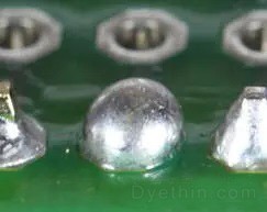
Too much solder
1) Possible causes:
The protruding lead length is too long, the flux is insufficient, the solder drag speed is too fast, and the nozzle peels off
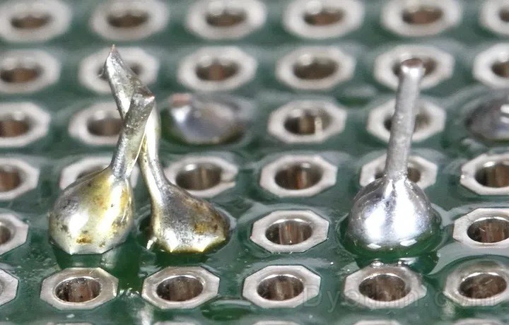
Too much solder
2) Solution
It is usually possible to remove some excess solder with the tip of a hot iron. In extreme cases, tin suckers or some solder cores can also help.
3) Preventive measures:
Reduce lead protrusion length, verify flux deposition, reduce drag speed, reprogram peel motion
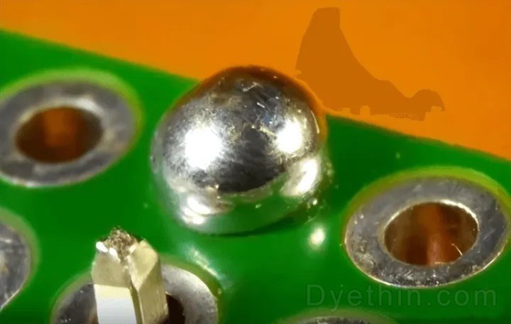
Too much solder
25. Joint overheating (hot welding)
The overheated solder joint is white, without metallic luster, and the surface is rough.
1) Possible causes
Because the soldering iron temperature is set too high
Solder cannot flow
It may be that there is already a layer of oxide on the surface of the pad or lead, preventing sufficient heat transfer
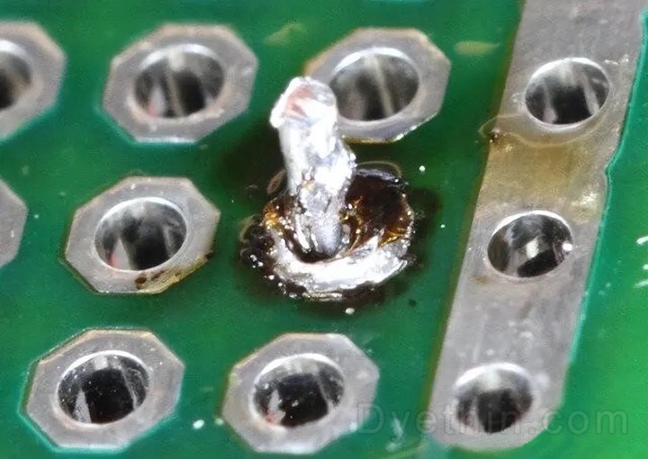
Burnt solder joint (more like burnt solder mask)
2) Solution
Overheated joints can usually be repaired after cleaning, scraped carefully with a knife tip, or a small amount of isopropanol and toothbrush will remove the scorched flux.
3) Prevention:
Clean hot soldering iron, correct soldering iron temperature and cleaning the joint with flux will help prevent the joint from overheating.
Articles you may also like
CR2025 Battery: Equivalent, Specifications and Replacements
Understanding Toggle Switches: A Comprehensive Guide
CR1632 vs CR2032: Are CR1632 and CR2032 battery equivalent?
CR1616 Battery Equivalent: Best Replacement Guide