













- 홈
- Blogs
- Basic knowledge
- Operational amplifier working principle and usage skills
Operational amplifier working principle and usage skills
An operational amplifier ("op amp" for short) is a circuit unit with a very high amplification factor. In actual circuits, some kind of functional module is usually combined with a feedback network. It is an amplifier with a special coupling circuit and feedback. Its output signal can be the result of mathematical operations such as addition, subtraction, or differentiation and integration of the input signal. It was named "operational amplifier" due to its early application in analog computers to realize mathematical operations.
Because it was used in analog computers in the early days to realize mathematical operations, it was named "operational amplifier". An operational amplifier is a circuit unit named from a functional point of view, which can be realized by a discrete device or in a semiconductor chip. With the development of semiconductor technology, most operational amplifiers exist in the form of a single chip. There are many types of operational amplifiers, which are widely used in the electronics industry.
Introduction
The operational amplifier is an electronic integrated circuit containing a multi-stage amplifier circuit. Its input stage is a differential amplifier circuit with high input resistance and the ability to suppress zero-point drift; the intermediate stage mainly performs voltage amplification and has a high voltage magnification. It is composed of a pole amplifier circuit; the output pole is connected to the load, which has the characteristics of strong load capacity and low output resistance. Operational amplifiers are used in a wide variety of applications.
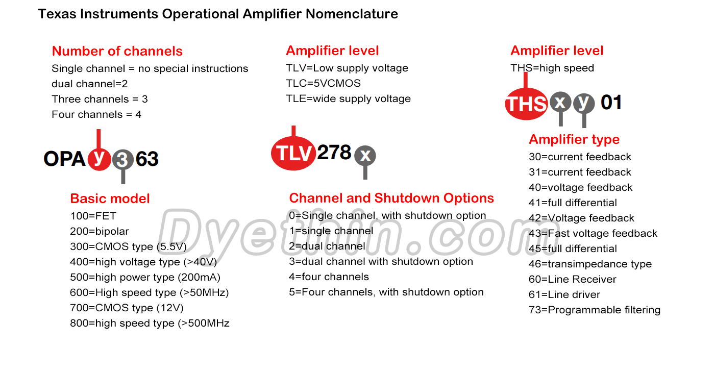
Texas Instruments Operational Amplifier Nomenclature
How Operational Amplifiers Work
1. Basic principles
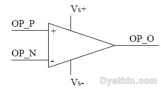
The operational amplifier has three ports, including two input ports, "+" and "-", and one output port. When the input signal is input into the amplifier from the "-" port, the output signal at the output port is opposite to the input signal; conversely, when the input signal is input into the amplifier from the "+" port, the output signal at the output port is in phase with the input signal; when the two input ports When the signals are input at the same time, the operational amplifier realizes the subtraction operation, and the output signal is in phase with the larger one. So an op amp is basically a voltage amplifier. An ideal operational amplifier must have the following characteristics: infinite input impedance, zero output impedance, infinite open-loop gain, infinite common-mode rejection ratio, and infinite bandwidth. A basic op amp is shown in Figure 1:
Basic Operational Amplifier
Basic operational amplifier
Usually, when an operational amplifier is used, its output terminal is connected to its inverting input node to form a negative feedback state. The reason is that the voltage gain of the operational amplifier is very large, ranging from hundreds to tens of thousands of times, and the use of negative feedback can ensure the stable operation of the circuit. But this does not mean that the operational amplifier cannot be connected as a positive feedback (positive feedback). On the contrary, in many systems that need to generate oscillating signals, an operational amplifier with a positive feedback configuration is a very common component.
2. Open loop circuit
The open-loop operational amplifier is shown in Figure 2. When an ideal operational amplifier operates in an open-loop manner, the relationship between its output and input voltage is as follows:
Vout=(V+-V-)*Aog
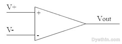
Open-loop operational amplifier
Among them, Aog represents the open-loop differential gain of the operational amplifier (open-loop differential gain). Since the open-loop gain of the operational amplifier is very high, even if the differential signal at the input terminal is small, the output signal will still be "saturated" (saturation) ), resulting in nonlinear distortion. Therefore, operational amplifiers rarely appear in circuit systems as open-loop circuits. A few exceptions are operational amplifiers used as comparators. The output of the comparator is usually "0" and "1" of the logic level.
3. Closed-loop negative feedback
Connect the inverting input terminal of the operational amplifier to the output terminal, and the amplifier circuit is in the state of negative feedback configuration. At this time, the circuit can usually be simply called a closed-loop amplifier. Closed-loop amplifiers can be divided into two types: inverting amplifiers and non-inverting amplifiers, depending on where the input signal enters the amplifier.
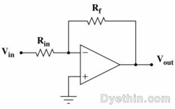
Inverting closed-loop amplifier
The inverting closed-loop amplifier is shown in Figure 3. Assuming that this closed-loop amplifier uses an ideal operational amplifier, since its open-loop gain is infinite, the two input terminals of the operational amplifier are virtual ground, and the relationship between the output and the input voltage is as follows:
Vout=-(Rf/Rin)*Vin
The non-inverting closed-loop amplifier is shown in Figure 4. Assuming that this closed-loop amplifier uses an ideal operational amplifier, because its open-loop gain is infinite, the voltage difference between the two input terminals of the operational amplifier is almost zero, and the relationship between the output and the input voltage is as follows:
Vout = ((R2/R1)+1)* Vin
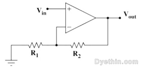
Non-inverting closed-loop amplifier
4. Closed-loop positive feedback
Connect the positive input terminal of the operational amplifier to the output terminal, and the amplifier circuit is in the state of positive feedback. Since the positive feedback configuration works in an extremely unstable state, it is mostly used in applications that need to generate oscillating signals.
The above is the introduction of the working principle of the operational amplifier. In practical applications, the selection of operational amplifiers must take into account the design purpose, target signal level, closed-loop gain, required accuracy, environmental conditions and other factors, and convert the required performance into the corresponding parameters of the operational amplifier. Although the operational amplifier circuit is difficult, no matter how complex the circuit is, as long as the basic characteristics of the operational amplifier circuit are grasped using appropriate methods, all problems can be answered.
Classification of Operational Amplifiers
1. General-purpose integrated operational amplifier
A general-purpose integrated operational amplifier means that its technical parameters are relatively moderate and can meet the usage requirements in most situations. General-purpose integrated operational amplifiers are divided into type I, type II and type III. Type I is a low-gain operational amplifier, type II is a medium-gain operational amplifier, and type III is a high-gain operational amplifier. Types I and II are basically early products, with input offset voltage around 2mV and open-loop gain generally greater than 80dB. The main characteristics of this type of device are low price, large product volume and wide range, and its performance indicators can be suitable for general use.
2. High precision integrated operational amplifier
High-precision integrated operational amplifiers refer to those operational amplifiers with small offset voltage, very small temperature drift, and very high gain and common-mode rejection ratio. These op amps are also less noisy. Among them, the offset voltage of a single high-precision integrated operational amplifier can be as small as a few microvolts, and the temperature drift can be as small as tens of microvolts per degree Celsius.
3. High-speed integrated operational amplifier
In fast A/D and D/A converters and video amplifiers, the conversion rate SR of the integrated operational amplifier must be high, and some can reach 2-3kV/μs. The unit gain bandwidth BWG must be large enough, as general-purpose integrated operational amplifiers are not suitable for high-speed applications. The main features of high-speed operational amplifiers are high slew rate and wide frequency response.
4. High Input Impedance Integrated Operational Amplifier
The input impedance of the high input impedance integrated operational amplifier is very large and the input current is very small. The input stage of this type of operational amplifier often uses MOS tubes.
5. Low power integrated operational amplifier
The working current of the low-power integrated operational amplifier is very small, and the power supply voltage is also very low. The power consumption of the entire operational amplifier is only tens of microwatts. This type of integrated operational amplifier is mostly used in portable electronic products. Since the biggest advantage of electronic circuit integration is to make complex circuits small and lightweight, as the application scope of portable instruments expands, operational amplifiers with low power supply voltage and low power consumption must be used.
6. Broadband Integrated Operational Amplifier
The wide-band integrated operational amplifier has a very wide frequency band, and its unity gain bandwidth can reach more than 1 gigahertz. It is often used in wide-band amplification circuits.
7. High-voltage integrated operational amplifier
The output voltage of the operational amplifier is mainly limited by the power supply. In ordinary operational amplifiers, the maximum output voltage is generally only a few tens of volts, and the output current is only a few tens of milliamperes. To increase the output voltage or increase the output current, an auxiliary circuit must be added outside the integrated operational amplifier. The high-voltage and high-current integrated operational amplifier can output high voltage and high current without any external circuitry. Generally, the power supply voltage of integrated operational amplifiers is below 15V, while the power supply voltage of high-voltage integrated operational amplifiers can reach tens of volts.
8. Power integrated operational amplifier
The output stage of the power integrated operational amplifier can provide relatively large power output to the load.
9. Low temperature drift operational amplifier
In automatic control instruments such as precision instruments and weak signal detection, it is always hoped that the offset voltage of the operational amplifier should be small and not change with changes in temperature. Low temperature drift op amps are designed for this purpose.
10. Programmable control operational amplifier
The issue of measuring range will be involved in the use of instruments. In order to obtain a fixed voltage output, the amplification factor of the operational amplifier must be changed
Professional terminology for operational amplifiers
Bandwidth Bandwidth: The frequency value when the voltage gain becomes low frequency 1/(2)
Common mode rejection ratio: common mode rejection ratio
Harmonic distortion: harmonic distortion The sum of the root mean square values of the harmonic voltage/the root mean square value of the fundamental voltage
Input bias current: input biascurrent is the average value of the current at the two input terminals.
Input voltage range: input voltage range Common mode voltage input range The voltage on the input terminal when the op amp is working normally;
Input impedance: input impendence Rs Rl is the ratio of input voltage to input current when specified.
Input offset current input offset current When the op amp outputs 0, the difference in current flowing into the two input terminals;
Input offset voltage input offsetvoltage In order to make the output 0, the voltage value added to the two input terminals through two equal-valued resistors
Input resistance: input resistance: any input terminal is grounded, the change value of the input voltage/the change value of the input current
Large-signal voltage gain: large-signal voltage gain output voltage swing/input voltage
Output impedance: output impendence Rs Rl is the ratio of the output voltage to the output current when specified.
Output resistance: output resistance output voltage is 0, small signal resistance seen from the output
Output voltage swing: outputvoltage swing The peak value of the voltage that can be input normally at the output of the op amp;
Offset voltage temperature drift offset voltage temperature drift
Power supply rejection ratio: power supply rejection input offset current change value/power supply change value
Settling time settlingtime is the time from the beginning of input to the output reaching stability;
Slew rate: slew rate The rate of change of the output terminal voltage when a large-scale step signal is applied to the input terminal
Supply current supply current
Transient response transient response small signal step response
Unity gain bandwidth unity gain bandwidth The frequency value when the open loop gain is 1
Voltage gain voltage gain refers to output voltage/input voltage when rs rl is fixed
The specific meaning of each parameter of the op amp
1. Input offset voltage
(Input Offset Voltage) VOS
If the two input terminals of the op amp are grounded, the output of the ideal op amp is zero, but the output of the actual op amp is not zero. At this time, the equivalent input voltage obtained by dividing the output voltage by the gain is called the input offset voltage. Its value is several mV, the smaller the value, the better, and the gain is limited when it is larger.
Input offset voltage VIO: The input offset voltage is defined as the compensation voltage applied between the two input terminals when the output terminal voltage of the integrated operational amplifier is zero. The input offset voltage actually reflects the symmetry of the circuit inside the op amp, the better the symmetry, the smaller the input offset voltage. Input offset voltage is a very important indicator of an op amp, especially when it is a precision op amp or used for DC amplification. The input offset voltage has a certain relationship with the manufacturing process. The input offset voltage of the bipolar process (that is, the above-mentioned standard silicon process) is between ±1~10mV; if a field effect transistor is used as the input stage, the input offset voltage will be larger. Some. For precision op amps, the input offset voltage is generally below 1mV. The smaller the input offset voltage, the smaller the mid-zero offset during DC amplification, and the easier it is to handle. Therefore, it is an extremely important indicator for precision operational amplifiers.
2. Temperature drift of input offset voltage
(Input Offset Voltage Drift)
Also called the temperature coefficient TC VOS, it is generally a few uV/.C. The temperature drift of the input offset voltage (referred to as the temperature drift of the input offset voltage) αVIO: The temperature drift of the input offset voltage is defined as the change of the input offset voltage within a given temperature range. The ratio of temperature changes. This parameter is actually a supplement to the input offset voltage, making it easy to calculate the drift of the amplifier circuit due to temperature changes within a given operating range. The input offset voltage temperature drift of general op amps is between ±10~20μV/℃, and the input offset voltage temperature drift of precision op amps is less than ±1μV/℃.
3. Input bias current
(Input Bias Current) IBIAS
The average value of the DC current flowing into or out of the two input terminals of the op amp. For bipolar op amps, this value has a large discreteness, but it is hardly affected by temperature; while for MOS op amps, this value is the gate leakage current, which is very small, but is greatly affected by temperature. Input bias current IIB: The input bias current is defined as the average bias current of the two input terminals when the output DC voltage of the op amp is zero. Input bias current has a great impact on high-impedance signal amplification, integration circuits and other places that require input impedance. The input bias current has a certain relationship with the manufacturing process. The input bias current of the bipolar process (that is, the above-mentioned standard silicon process) is between ±10nA~1μA; if a field effect transistor is used as the input stage, the input bias current Typically less than 1nA.
4. Input offset current
(Input Offset Current) IOS
It is the absolute value of the difference between the input bias currents at the two input terminals of the op amp.
Input offset current IIO: The input offset current is defined as the difference in the bias current of the two input terminals when the output DC voltage of the op amp is zero. The input offset current also reflects the circuit symmetry inside the op amp. The better the symmetry, the smaller the input offset current. Input offset current is a very important indicator of an op amp, especially when it is a precision op amp or used for DC amplification. The input offset current is approximately one percent to one tenth of the input bias current. Input offset current has an important impact on small-signal precision amplification or DC amplification. Especially when a larger resistor is used outside the op amp (for example, 10kΩ or more), the input offset current may have a greater impact on accuracy than the input offset voltage. Impact. The smaller the input offset current, the smaller the mid-zero offset during DC amplification, and the easier it is to handle. Therefore, it is an extremely important indicator for precision operational amplifiers.
5. Input resistance Rin
The differential input resistance between the two input terminals of an op amp.
This value is defined by a tiny AC signal, and the actual impact is so small that it can be ignored. The common-mode input resistance at the input of the op amp is 10-1000 times that of Rin, which is also negligible.
6. Voltage gain AV
Also called differential voltage gain. The AV of an ideal op amp is infinite, and the actual op amp is generally about hundreds of dB.
Differential mode open-loop DC voltage gain: Differential mode open-loop DC voltage gain is defined as the ratio of the op amp output voltage to the differential mode voltage input voltage when the op amp operates in the linear region. Since the differential mode open-loop DC voltage gain is very large, the differential mode open-loop DC voltage gain of most operational amplifiers is generally tens of thousands times or more. It is inconvenient to compare directly with numerical values, so decibels are generally used to record and compare. Generally, the differential-mode open-loop DC voltage gain of an operational amplifier is between 80 and 120dB. The differential-mode open-loop voltage gain of an actual op amp is a function of frequency, and for ease of comparison, the differential-mode open-loop DC voltage gain is generally used.
7. Maximum output voltage VOM
The output voltage before saturation is called the maximum output voltage, and an ideal op amp can reach full-scale (rail to rail) output.
8. Common mode input voltage range CMVR
(Input Common-Mode Voltage Range) VICM
Indicates the range of common-mode voltage that can be applied between the two input terminals of the op amp and the ground. It is an ideal characteristic when VICM is equal to the positive and negative power supply voltages, and the full-scale output op amp is close to this characteristic.
9. Common mode signal rejection ratio
(Common Mode Rejection Ratio) CMRR
When the same signal is applied between the two input terminals of the operational amplifier and the ground, the gain between the input and the output is called the common-mode voltage gain AVC, and the CMRR is defined as:
CMRR =AV/AVC
Common-mode rejection ratio: The common-mode rejection ratio is defined as the ratio of the differential-mode gain of the op amp to the common-mode gain when the op amp is operating in the linear region. The common-mode rejection ratio is an extremely important indicator, which can suppress the differential-mode input==mode interference signal. Since the common mode rejection ratio is very large, the common mode rejection ratio of most op amps is generally tens of thousands times or more. It is inconvenient to directly express it with numerical values, so it is generally recorded and compared in decibels. The common mode rejection ratio of general operational amplifiers is between 80 and 120dB.
10. Power supply voltage rejection ratio
(Supply Voltage Rejection Ratio) SVRR
As the positive and negative supply voltages vary, that change appears at the output of the op amp and is scaled to the value at the input of the op amp. If the equivalent input conversion voltage is ΔVin when the power supply changes ΔVs, then SVRR is defined as:
SVRR = ΔVs/ΔVin
Power supply voltage rejection ratio: The power supply voltage rejection ratio is defined as the ratio of the op amp input offset voltage changing with the power supply voltage when the op amp operates in the linear region. The supply voltage rejection ratio reflects the impact of power supply changes on the output of the op amp. At present, the power supply voltage rejection ratio can only be about 80dB. Therefore, when used for DC signal processing or small signal processing analog amplification, the power supply of the op amp needs to be carefully and carefully processed. Of course, an op amp with a high common-mode rejection ratio can compensate for part of the power supply voltage rejection ratio. In addition, when dual power supplies are used, the power supply voltage rejection ratios of the positive and negative power supplies may be different.
11. Current consumption ICC
This current refers to the current flowing through the power supply terminal of the op amp, which changes with the external circuit and power supply voltage.
12. Slew Rate SR
Indicates the degree to which the op amp can track how fast the input signal changes. The unit is V/us.
Slew rate (also called slew rate) SR: The slew rate of an op amp is defined as when a large signal (including a step signal) is input to the input of the op amp when the op amp is connected in a closed loop. The output rise rate of the op amp is measured at the terminal. Since the op amp's input stage is on and off during conversion, the op amp's feedback loop is inactive, meaning that the slew rate is independent of the closed-loop gain. The conversion rate is a very important indicator for large signal processing. For general operational amplifiers, the conversion rate is SR<=10V/μs, and for high-speed operational amplifiers, the conversion rate is SR>10V/μs. The current maximum conversion rate SR of high-speed operational amplifiers reaches 6000V/μs. This is used for op amp selection in large signal processing.
13. Gain bandwidth product
(Gain Bandwidth Product) GB
Parameter representing the voltage gain-frequency characteristic of the op amp, unit is MHz.
Unit gain bandwidth GB: Unit gain bandwidth is defined as, when the closed-loop gain of the operational amplifier is 1 times, a small constant-amplitude sinusoidal signal is input to the input terminal of the operational amplifier, and the closed-loop voltage gain measured from the output terminal of the operational amplifier drops by 3db. (or the signal frequency corresponding to 0.707 of the op amp input signal). Unit gain bandwidth is a very important indicator. For sinusoidal small signal amplification, unit gain bandwidth is equal to the product of the input signal frequency and the maximum gain at that frequency. In other words, when the frequency of the signal to be processed and the signal required are known After increasing, the unity gain bandwidth can be calculated to select the appropriate op amp. This is used for op amp selection in small signal processing.

Articles you may also like
CR2025 Battery: Equivalent, Specifications and Replacements
Understanding Toggle Switches: A Comprehensive Guide

CR1616 Battery Equivalent: Best Replacement Guide

CR1632 vs CR2032: Are CR1632 and CR2032 battery equivalent?

-
-
-
-
-
-
-
broadcom-limited
-
-