


- Home
- Featured Products
- Nexperia
- 74HC595D Pinout, Timing, and SO16 Package Guide
74HC595D Pinout, Timing, and SO16 Package Guide
Overview of the 74HC595D Shift Register
The 74HC595D is an 8-bit shift register designed to accept serial input and provide either serial or parallel output. It is particularly suited for expanding output capabilities in microcontroller-based systems. Unlike conventional parallel I/O expanders, the 74HC595D integrates a separate latch register, enabling output data to be stored and updated independently of the shift operation.
One of the defining characteristics of the 74HC595D is its dual clock configuration, which allows data to be shifted in on one clock edge and latched on another. This mechanism provides flexibility in timing control and prevents unwanted glitches on the output pins. The chip includes an output enable control that can set all outputs to high impedance, making it ideal for bus sharing scenarios.
With the ability to cascade multiple 74HC595D devices via its serial output (Q7S), this register becomes a powerful tool for building large display arrays, keypad scanners, and LED drivers, all while using minimal microcontroller pins.
Key Features and Electrical Advantages

The 74HC595D offers efficient performance for serial-to-parallel data applications. Designed for a wide supply voltage range from 2V to 6V, it supports both CMOS logic levels for the HC version and TTL levels for the HCT variant. This flexibility makes the 74HC595D suitable for integration in a variety of logic families without the need for level shifting.
With an operating frequency up to 100 MHz (typical), the 74HC595D ensures high-speed data transfer in timing-critical systems. The internal structure features an 8-bit shift register and a storage register with 3-state outputs. These outputs can be placed in a high-impedance state when not in use, making the device ideal for shared output buses or display multiplexing.
Another benefit of the 74HC595D is its built-in clamp diodes at all inputs, which allow interfacing with signals above VCC when current-limiting resistors are applied. Additionally, it supports latch-up immunity exceeding 100 mA, and ESD protection levels meet standard JEDEC Class 2 ratings, improving its robustness in harsh environments.
Common Applications of 74HC595D
The 74HC595D is frequently used to expand output capabilities in systems with limited I/O lines. By shifting data serially and outputting it in parallel, this register minimizes the number of microcontroller pins required to drive multiple outputs. A common use case is controlling LED matrices, where each output pin from the 74HC595D manages one LED or segment.
In embedded systems, the 74HC595D helps drive numeric displays, such as 7-segment or multi-digit LCD modules, allowing efficient multiplexing. It is also widely applied in industrial equipment where multiple status indicators or control lines must be handled with limited GPIO resources.
Another popular application of the 74HC595D is in digital audio or MIDI controllers, where multiple button states or switch positions need to be latched and managed in sync. The ability to cascade several 74HC595D chips makes it ideal for scalable panel designs without redesigning the core controller.
Package Types and Ordering Codes

74HC595D SO16 Package Pinout
| Pin Number | Pin Name | Function |
|---|---|---|
| 1 | Q1 | Parallel output bit 1 |
| 2 | Q2 | Parallel output bit 2 |
| 3 | Q3 | Parallel output bit 3 |
| 4 | Q4 | Parallel output bit 4 |
| 5 | Q5 | Parallel output bit 5 |
| 6 | Q6 | Parallel output bit 6 |
| 7 | Q7 | Parallel output bit 7 |
| 8 | GND | Ground |
| 9 | Q7S | Serial data output (for cascading) |
| 10 | MR | Master reset (active LOW) |
| 11 | SHCP | Shift register clock input |
| 12 | STCP | Storage register clock input |
| 13 | OE | Output enable (active LOW) |
| 14 | DS | Serial data input |
| 15 | Q0 | Parallel output bit 0 |
| 16 | VCC | Supply voltage |
The 74HC595D is offered in multiple package formats to meet different layout and space requirements. One of the most common options is the SO16 package, which is well-suited for standard through-hole replacement in compact boards. For applications where board space is limited, the TSSOP16 and QFN packages provide smaller footprints without compromising electrical performance.
Each version of the 74HC595D is identified by a unique suffix in the part number. For example, ordering codes like 74HC595PW or 74HC595BQ correspond to TSSOP and QFN variants respectively. These identifiers ensure compatibility with automated assembly processes and allow designers to match the package type to their mechanical constraints.
Functional Block Diagram Explained

The internal structure of the 74HC595D is built around two main sections: an 8-bit serial-in shift register and an 8-bit storage register. Data enters through the DS pin and is shifted through the register on the rising edge of the shift clock (SHCP). This allows bits to be loaded one at a time while maintaining precise timing control.
Once the data is fully shifted, a separate latch clock (STCP) transfers the contents from the shift register to the storage register. This mechanism ensures that output states change only when intended, avoiding glitches during shifting. The outputs Q0 to Q7 reflect the values stored in the storage register when the OE pin is active (logic low).
The 74HC595D also features a serial output (Q7S), enabling multiple devices to be daisy-chained. This is useful when expanding the number of outputs without increasing microcontroller pin usage. These combined functions make the 74HC595D ideal for LED drivers, multiplexed displays, and digital control panels.
Pin Configuration and Function Descriptions
The 74HC595D comes in a 16-pin layout, with each pin assigned a dedicated function for shifting, latching, output control, or power management. Pins Q0 to Q7 serve as parallel data outputs, which reflect the contents of the internal storage register. The DS pin is used to input serial data, which gets shifted in on each clock pulse applied to SHCP.
The STCP pin controls when data from the shift register is latched into the output register, making the timing of this signal critical for synchronized output updates. The OE pin enables or disables all outputs, placing them in a high-impedance state when set high. The MR pin clears the shift register asynchronously when pulled low, without affecting the storage register.
The 74HC595D also features a Q7S pin that outputs the last bit of the shift register, allowing multiple 74HC595D chips to be cascaded. VCC and GND supply power and ground, respectively, and must be connected appropriately for stable operation.
How Data Shifting and Storage Works

Figure Reference: Logic diagram
The 74HC595D manages data using two distinct but synchronized registers. Data enters the chip serially through the DS input. Each rising edge of the SHCP clock causes the bit stream to shift one position through the 8-bit shift register. This mechanism builds the data word from LSB to MSB over consecutive clock pulses.
Once all bits are shifted in, the STCP clock pulse copies the contents of the shift register into the internal storage register. The storage register then controls the outputs Q0 to Q7. This separation ensures that output data remains stable while new serial data is being loaded, which is essential in timing-sensitive circuits.
The 74HC595D allows chaining by outputting the last shift register bit through Q7S. This output can feed into the DS input of a second 74HC595D, enabling multi-byte output expansion with just three control lines. In digital control applications such as multiplexed displays, this approach makes the 74HC595D an efficient option.
Absolute Maximum Ratings
The 74HC595D is rated for operation in a broad electrical range, but exceeding certain thresholds may cause permanent damage. The maximum supply voltage (VCC) must not exceed 7V. Signals applied to any input pin must stay within -0.5V to VCC + 0.5V to prevent excessive current through the internal protection diodes.
Each output pin can source or sink limited current, typically up to ±35 mA for the parallel Qn outputs and ±25 mA for the serial output Q7S. However, the total current into or out of the ground or supply pins should not exceed 70 mA. To maintain device integrity, the 74HC595D must also operate within a storage temperature range of -65°C to +150°C.
Designers using the 74HC595D in high-density or thermally constrained environments should be aware of the total power dissipation limits, which vary by package type. Thermal derating applies beyond specified junction temperatures and must be considered during layout and system-level thermal design.
Absolute Maximum Ratings

The 74HC595D is rated for operation in a broad electrical range, but exceeding certain thresholds may cause permanent damage. The maximum supply voltage (VCC) must not exceed 7V. Signals applied to any input pin must stay within -0.5V to VCC + 0.5V to prevent excessive current through the internal protection diodes.
Each output pin can source or sink limited current, typically up to ±35 mA for the parallel Qn outputs and ±25 mA for the serial output Q7S. However, the total current into or out of the ground or supply pins should not exceed 70 mA. To maintain device integrity, the 74HC595D must also operate within a storage temperature range of -65°C to +150°C.
Designers using the 74HC595D in high-density or thermally constrained environments should be aware of the total power dissipation limits, which vary by package type. Thermal derating applies beyond specified junction temperatures and must be considered during layout and system-level thermal design.
Timing Characteristics and Propagation Delays

Figure Reference: Shift clock pulse, maximum frequency and input to output propagation delays
The 74HC595D is optimized for high-speed data operations and supports fast signal propagation across its internal registers. When operating at 4.5V, typical delays from the shift clock (SHCP) to the serial output (Q7S) range around 19ns. Similarly, the delay from the latch clock (STCP) to the parallel outputs (Q0–Q7) is typically 20ns under the same voltage conditions.
Timing behavior of the 74HC595D is consistent across a wide temperature range, which ensures signal stability in industrial and automotive systems. The 74HC595D can operate at a maximum shift frequency of approximately 100 MHz (typical), though actual performance depends on voltage and load conditions. Signal rise and fall times are sharp, contributing to precise timing control in high-speed applications.
When using the 74HC595D in cascaded configurations, designers must account for cumulative delays, especially between SHCP and STCP transitions. These delays directly affect data synchronization across multiple devices. Understanding the timing chart and test circuit conditions is critical when integrating the 74HC595D into clock-sensitive applications.
Package Drawings and Mechanical Dimensions

Figure Reference: SO16
The 74HC595D is commonly supplied in the SO16 package, identified as SOT109-1. This format features a 3.9 mm body width and a 1.27 mm pin pitch, making it suitable for standard PCB designs and compatible with most surface-mount production lines. The SO16 package includes 16 leads arranged in two rows, offering a straightforward layout for routing parallel outputs and control signals.
Engineers selecting the 74HC595D for applications such as LED driving, signal expansion, or general digital control will find the SO16 outline convenient for both prototyping and high-volume assembly. The consistent pin spacing and overall dimensions ensure reliable solder joint formation and mechanical stability under standard reflow profiles.
Related articles
CR2430 Battery Replacements, Equivalents, and Applications
CR2025 Battery: Equivalent, Specifications and Replacements
FAQs
Articles you may also like
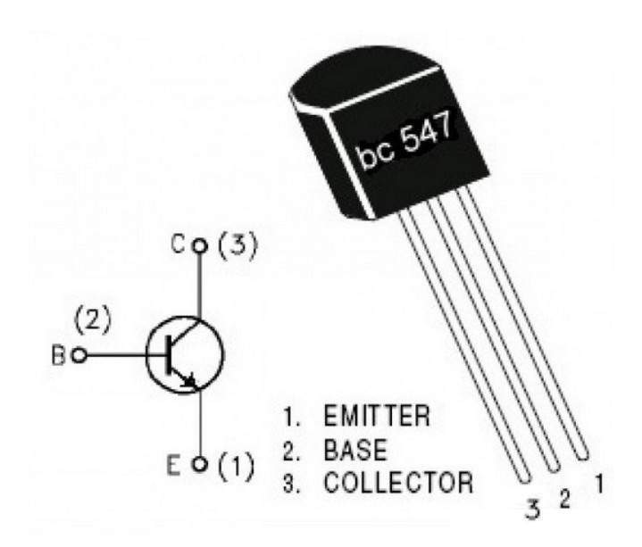
BC547 NPN transistor usage case and explanation of BC547 Datasheet and BC547 pinout
BAV99 datasheet and BAV99 pinout,Differences from TVS tubes
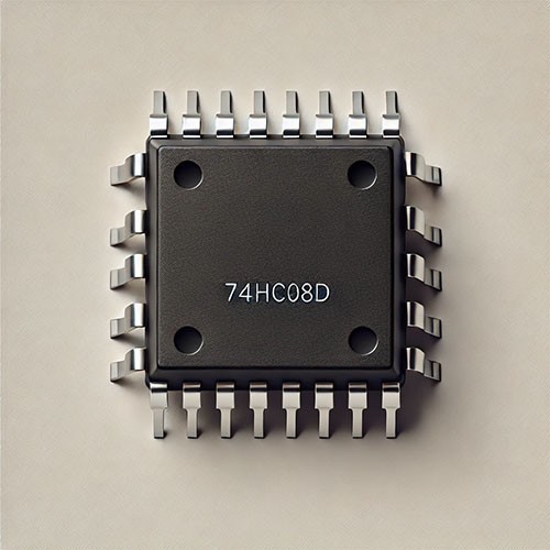
Nexperia 74HC08D Quad 2-Input AND Gate
NX3008NBK MOSFET: Features, Applications, and Design Guide
Inventory Quantity: 8,927


